Design of Ultra High-Speed CMOS CML buffers and Latches
advertisement

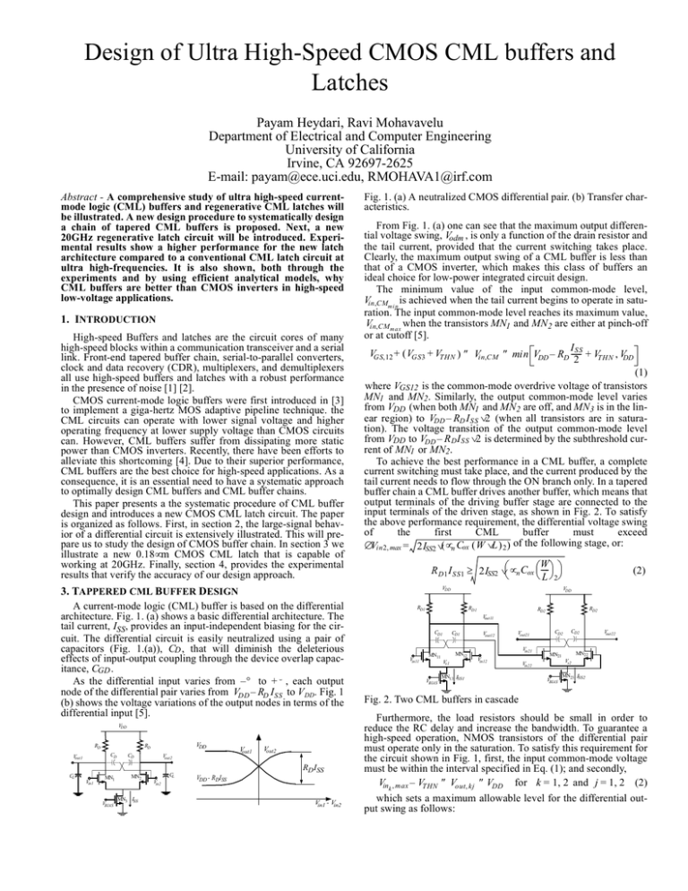
Design of Ultra High-Speed CMOS CML buffers and Latches Payam Heydari, Ravi Mohavavelu Department of Electrical and Computer Engineering University of California Irvine, CA 92697-2625 E-mail: payam@ece.uci.edu, RMOHAVA1@irf.com Abstract - A comprehensive study of ultra high-speed currentmode logic (CML) buffers and regenerative CML latches will be illustrated. A new design procedure to systematically design a chain of tapered CML buffers is proposed. Next, a new 20GHz regenerative latch circuit will be introduced. Experimental results show a higher performance for the new latch architecture compared to a conventional CML latch circuit at ultra high-frequencies. It is also shown, both through the experiments and by using efficient analytical models, why CML buffers are better than CMOS inverters in high-speed low-voltage applications. 1. INTRODUCTION High-speed Buffers and latches are the circuit cores of many high-speed blocks within a communication transceiver and a serial link. Front-end tapered buffer chain, serial-to-parallel converters, clock and data recovery (CDR), multiplexers, and demultiplexers all use high-speed buffers and latches with a robust performance in the presence of noise [1] [2]. CMOS current-mode logic buffers were first introduced in [3] to implement a giga-hertz MOS adaptive pipeline technique. the CML circuits can operate with lower signal voltage and higher operating frequency at lower supply voltage than CMOS circuits can. However, CML buffers suffer from dissipating more static power than CMOS inverters. Recently, there have been efforts to alleviate this shortcoming [4]. Due to their superior performance, CML buffers are the best choice for high-speed applications. As a consequence, it is an essential need to have a systematic approach to optimally design CML buffers and CML buffer chains. This paper presents a the systematic procedure of CML buffer design and introduces a new CMOS CML latch circuit. The paper is organized as follows. First, in section 2, the large-signal behavior of a differential circuit is extensively illustrated. This will prepare us to study the design of CMOS buffer chain. In section 3 we illustrate a new 0.18µm CMOS CML latch that is capable of working at 20GHz. Finally, section 4, provides the experimental results that verify the accuracy of our design approach. 3. TAPPERED CML BUFFER DESIGN A current-mode logic (CML) buffer is based on the differential architecture. Fig. 1. (a) shows a basic differential architecture. The tail current, ISS, provides an input-independent biasing for the circuit. The differential circuit is easily neutralized using a pair of capacitors (Fig. 1.(a)), CD , that will diminish the deleterious effects of input-output coupling through the device overlap capacitance, CGD . As the differential input varies from – ∞ to + ∞, each output node of the differential pair varies from VDD – RD ISS to V DD. Fig. 1 (b) shows the voltage variations of the output nodes in terms of the differential input [5]. VDD RD CL Vin1 VDD RD CD Vout1 MN1 VBIAS CD MN2 MN3 ISS Vout2 CL Vin2 Vout1 Vout2 RD ISS VDD - RDISS Vin1 - Vin2 Fig. 1. (a) A neutralized CMOS differential pair. (b) Transfer characteristics. From Fig. 1. (a) one can see that the maximum output differential voltage swing, Vodm , is only a function of the drain resistor and the tail current, provided that the current switching takes place. Clearly, the maximum output swing of a CML buffer is less than that of a CMOS inverter, which makes this class of buffers an ideal choice for low-power integrated circuit design. The minimum value of the input common-mode level, Vin ,CMmi n is achieved when the tail current begins to operate in saturation. The input common-mode level reaches its maximum value, Vin, CM max when the transistors MN1 and MN2 are either at pinch-off or at cutoff [5]. I SS - + VTHN , VDD VGS, 12 + ( VGS3 + VTHN ) ≤ Vin,C M ≤ min VDD – RD ----2 (1) where VGS12 is the common-mode overdrive voltage of transistors MN1 and MN2. Similarly, the output common-mode level varies from VDD (when both MN1 and MN2 are off, and MN3 is in the linear region) to VDD – RD I SS ⁄ 2 (when all transistors are in saturation). The voltage transition of the output common-mode level from VDD to VDD – R D I SS ⁄ 2 is determined by the subthreshold current of MN1 or MN2. To achieve the best performance in a CML buffer, a complete current switching must take place, and the current produced by the tail current needs to flow through the ON branch only. In a tapered buffer chain a CML buffer drives another buffer, which means that output terminals of the driving buffer stage are connected to the input terminals of the driven stage, as shown in Fig. 2. To satisfy the above performance requirement, the differential voltage swing of the first CML buffer must exceed ∆Vin2, max = 2ISS2 ⁄ ( µn Cox ( W ⁄ L ) 2 ) of the following stage, or: W R D1 I SS1 ≥ 2ISS2 ⁄ µ n Cox ----- L 2 VDD (2) VDD RD1 RD1 RD2 RD2 Vout11 CD1 Vin11 CD1 MN12 MN11 Vs1 VBIAS Vout12 Vout21 Vin21 Vin12 MN13 ISS1 CD2 CD2 Vout22 MN22 MN21 Vs2 Vin22 VBIAS MN23 ISS2 Fig. 2. Two CML buffers in cascade Furthermore, the load resistors should be small in order to reduce the RC delay and increase the bandwidth. To guarantee a high-speed operation, NMOS transistors of the differential pair must operate only in the saturation. To satisfy this requirement for the circuit shown in Fig. 1, first, the input common-mode voltage must be within the interval specified in Eq. (1); and secondly, Vink , max – VTHN ≤ Vout, kj ≤ VDD for k = 1, 2 and j = 1, 2 (2) which sets a maximum allowable level for the differential output swing as follows: for k = 1, 2 (3) RDk ISSk ≤ VTHN In addition, a high-speed CML output driver must drive a large off-chip load through the bondwire and package trace. The output driver must thus have a large current drive capability. This means that NMOS transistors of the second CML buffer in Fig. 2 must be large. A large transistor has a large gate-to-channel capacitance that seriously degrades the propagation delay and the voltage swing of the preceding predriver stage. To reduce the propagation delay of the predriver, a chain of tapered buffers is introduced between the first predriver stage and the second buffer. The minimum delay is obtained by dividing the delay equally over all stages. This is achieved by gradually scaling up all stages with a constant taper factor, u. On the other hand, the chip package interface at very high frequencies is appropriately modeled as a transmission line that is terminated by a load impedance, which is a series RC circuit (cf. Fig. 3). The series load resistance, Z0, provides the high-frequency parallel matched termination to the bondwire. Fig. 3 shows the schematic of the output CML driver driven by N-1 tapered CML buffers along with the chip-package interface being modeled as the transmission line. The drain resistor, RDN , of the last output CML buffer is determined by the series impedance matching to bondwire’s characteristic impedance. Subsequently, ISSN of the last driver stage is calculated using the output differential voltage swing and RD . The only remaining parameter in the last CML driver left is the (W/L) of the source-coupled transistor pair, which is obtained from the common-mode characteristic of the last CML buffer. If the commonmode input voltage lies in the allowable range given by Eq. (1), then the tail current is equally divided between the two branches of the differential stage, i.e., W- ( Vin , CM – Vsk – VTHN ≥ Vin , CM – VBIAS –2VTHN ) = ISSk ⁄ µ n Cox ---L k k k for k = 1, 2, ..., N (5) where Vin k , C M is the common-mode input voltage of the kth driver in the buffer chain. Vin k, C M is specified by the output commonmode voltage of the previous stage. Given a tapered buffer chain with a constant differential voltage swing, the maximum (W/L) of the transistor pair of the kth CML buffer is then calculated by solving Eq. (6): VDD RDN RDN CDN MNN1 ... 1 u uN-1 VBIAS Z0 CDN MNN2 Z0 CL Z0 CL Z0 MNN3 ISSN Fig. 3. An output CML buffer driving off-chip loads. The chippackage interface is electrically modeled using a lossless transmission line. The chip bondwires exhibit high-Q inductances. Therefore it is safe to model the chip-package interface using a lossless transmission line. To avoid potentially disastrous transmission line effects such as slow ringing and propagation delays, the bondwires are terminated both at the source using a series termination (RDN = Z0), and at the destination using a parallel termination (Z0). Given a well-defined output voltage swing (RD ISS) and with RD being determined by the matched termination, the tail current ISSN is easily calculated. For instance, an output differential voltage swing of 0.4V for a 50Ω line driver requires a bias current of 8mA. Now, using a set of constraints, we present design guidelines to design a tapered CML buffer chain and determine appropriate values for the circuit components of the CML buffer. The propagation delay is computed using the open-circuit time constant method [6]. For instance, the delay of the simple low-voltage differential stage of Fig. 1 (a) is 0.69RD CL. Various HSPICE simulations on high-speed CML buffers show that the delay obtained by the open-circuit time-constant method is within 8% of the actual simulation. Minimizing the overall propagation delay of CML buffer increases the overall operation frequency of the buffer significantly. For a slowly varying input signal, increasing the small-signal voltage gain will further decrease the output transient variations and the output transition time. In a chain of tapered CML buffers, to attain a constant voltage swing, transistor sizes are scaled up while the drain resistances are scaled down with a constant scaling factor. This will lead us to the fact that small-signal voltage gains of all constituting stages of the buffer chain are identical. W W W µn Cox ----- ISS1 RD1 = µn Cox ----- ISS2 RD2= … = µn Cox ----- ISS RD L 1 L 2 L As a consequence, Eq. (5) provides us with a lower bound for the maximum small-signal voltage gain at equilibrium, that is: W A = µn Cox ----- ISS RD ≥ 2 (4) v, eq L ISS ----- - – VBIAS – 2VTHN = ISS k ⁄ µ n Cox W (6) VDD – RD ---- L k 2 In the above equation RD I SS is the constant differential output swing of a tapered CML buffer chain. As mentioned above, in a chain of tapered CML buffers, the minimum delay is obtained by dividing the delay equally over all stages. However, the question is how many buffer stages are required to achieve the optimum delay. To answer this question, the propagation delay of an arbitrarily chosen CML stage in a buffer chain is first derived. Fig. 4 shows the kth stage in a chain of N tapered stages driving another CML stage along with the capacitors that contribute to the delay calculation. The common node sk+1 shown in Fig. 4 undergoes a smaller variation compared to the voltage variations of the input terminals particularly in a matched differential pair. In fact, it is easily shown that for a maximum differential input variation of ∆Vin, max, the maximum variation of the common node is ∆Vin, max ⁄ 2 . Therefore, the equivalent capacitance seen at the common node sk+1 is approximately Cs, k + 1 = 2 CDBS, k + 1 rather than CDBS, k + 1. The 50% delay of the kth stage is as follows: t d, k = 0.69RD, k (CDB, k s Cs, k + CGS, k + 1 s Cs, k + 1 ) (7) where s represents the series connection of electrical elements. The total propagation delay of the buffer chain is readily calculated: ∑t N td = d, k = 0.69NRD1 (CDB1 s Cs1 + X k=1 VDD CGS1 s Cs1 ) (8) VDD RD,k RD,k+1 RD,k CD,k 1⁄N RD,k+1 CD,k+1 CD,k+1 CD,k Vin,k+1,1 CDB,k CDB,k Vin,k+1,2 CGS,k+1 CGS,k+1 Vs,k+1 VBIAS CDBS,k VBIAS CDBS,k+1 Fig. 4. The kth and (k+1)st stages of a tapered CML buffer along with the parasitic capacitances Interestingly, the functional dependence between delay and the number of stages (or taper factor) is similar to the one in a CMOS buffer chain [7]. To be more specific, consider a chain of tapered CML buffers driving a lossless transmission line with a characteristic impedance of Z0. Suppose that the gate aspect-ratio of the transistor pair of the last CML line driver is X times larger than that of the first predriver stage. It is easily proved that if CDB1 = γ Cs1 and CGS1 = η Cs1 ; then it is easily proved that the optimum number of stages will be the numerical solution to the following equation: 1 ⁄ N o pt γ⁄η 1 ----------- + ------------- X 1 + γ 1 + η = exp -----------------------------------------------------(9) X 1 1 ⁄ Nop t ------------ X 1 + η or in the special case, if CDB1<<CGS1 then, Nopt = ln ( X ) which is well-known result. To further increase the bandwidth (reduce the delay), the intermediate stages use inductive peaking as demonstrated in Fig. 5. 1 ⁄ N opt VDD latch in Fig. 6, that lead to a complete operation failure at very highfrequencies ( ≥ 10GHz ). The primary limitation is that a single tail current is used for both tracking and latch circuits. Consequently, the bias operations of tracking and latch circuits are tightly related. This will severely limit the allowable transistor sizes for a reliable latch operation. At ultra high-frequencies ( ≥ 10GHz ) the parasitic capacitances of transistors, MN1 and MN2, degrade the required minimum gain for a proper tracking operation (Eq. (4)). Therefore, the tail current must be sufficiently high to achieve a wider range of linearity and a larger transconductance. On the other hand, the latch circuit does not need a large bias current at ultra high-frequencies. To address the aforementioned problems, the regenerative CML latch is modified so that the latch circuit and the tracking circuit use two distinct tail currents. Fig. 7 shows the new CML latch circuit. VDD RD1 RD1 RD2 RD2 VDD VDD Vout RD1 RD1 CD1 Vin11 Vout11 ..... CD1 V out12 ..... MN12 MN11 Vs1 VBIAS RDi RDi LD,i-1 LD,i-1 CD2 Vout,N1 Vin12 MNi1 Vin,i1 Vsi MN13 ISS1 VBIAS Vin,i2 CDN CDN Vout,N2 VBIAS MNN3 ISSN 3. ULTRA HIGH-SPEED LATCH DESIGN A current-mode logic (CML) latch consists of an input tracking stage, MN1 and MN2, utilized to sense and track the data variation and a cross-coupled regenerative pair, MN3 and MN4, being employed to store the data. Fig. 6 demonstrates a CMOS CML latch circuitry. VDD RD Vout Vin MN4 MN3 MN2 MNN6 MNN5 VCLK VCLK VBIAS MNN8 ISS2 ISS1 VsN Vin,N2 MNi3 ISSi The addition of the inductor in series with the drain resistor delays the current flow through the branch containing the resistor, making more current available for charging the device capacitors, and reducing the rise and fall times. From another perspective, the addition of an inductance in series with the load capacitance introduces a zero in the transfer function of the CML stage which helps offset the roll-off due to parasitic capacitances. Inductive peaking can increase the bandwidth to about 1.72 times larger than the unpeaked case [6]. Inductance values are scaled with the same taper factor as the drain resistors are. MN1 MNN7 VCLK MNN2 MNN1 Fig. 5. Multiple stage CML buffers along with the inductive peaking RD MNN6 MNN5 MN4 MN3 VREF VCLK Vin,N1 MNi2 MN2 MN1 Vin ..... ..... CD2 RDN RDN Fig. 7. The circuit schematic of the new CMOS CML latch circuit. As observed in Fig. 7, the tracking stage and the latch stage are now separately optimized for a correct latch operation at ultra high-frequencies. Note that it is important the source coupled pair transistors have high gain. This is obviously achieved with larger W ⁄ L for each transistor of the cross-coupled pair. However, this technique greatly limits the driving capability. Therefore the CML latch is followed by a CML buffer to recover the logic level. 4. EXPERIMENTAL RESULTS In this section the performance of the CML buffer is evaluated by performing experiments on single stage as well as multiple stages of the buffer. Experiments are set up to show the performance of the new CML latch depicted in Fig. 7 at 20GHz data-rate. First, the accuracy of Eq. (9) is verified by running HSPICE simulation on a chain of CML buffers. Then, the performance of the circuit in Fig. 7 is compared with the conventional CML latch shown in Fig. 6. 4.1. Tapered CML buffer experiment Similar to a CMOS tapered buffer, a single CML buffer might not be sufficient to drive an off-chip load. There are, however, more design trade-offs involved in the design of a CML tapered buffer than in a CMOS tapered buffer. A superior high-frequency performance in a CML buffer is guaranteed only if the design guidelines explained thoroughly in Section 2 to be taken into consideration. Fig. 8 plots propagation delay as a function of number of CML stages for different values of X, where X is the ratio between the off-chip load impedance and the load impedance of the first predriver stage. In practice, X is between 30-100. −10 MNN7 I SS 2.5 The track and latch modes are determined by the clock signal inputs to a second differential pair, MN5 and M N6. When the signal VCLK is "HIGH", the tail current ISS entirely flows to the tracking circuit, MN5 and M N6 , thereby allowing Vout to track Vin. In the latch-mode, the signal VCLK goes low, the tracking stage is disabled, whereas the latch pair is enabled storing the logic state at the output. Like CML buffers, a CML latch operates with relatively small voltage swings which is 4VTHN peak-to-peak differential-mode. Fig. 6 allows us to implement high-speed latch circuit. However, there are several shortcomings involved in the design of the regenerative Propagation Delay (sec) Fig. 6. the circuit schematic of a CMOS CML buffer. x 10 2 1.5 X = 80 X = 50 X = 30 X = 20 X = 10 1 0.5 0 1 2 3 4 Number of Stages (N) 5 6 Fig. 8. Delay vs. number of stages for CML tapered buffer chain. The delay variation in terms of the number of stages for CML tapered buffer and CMOS tapered buffer are almost identical. However, the total propagation delay of a CML buffer chain for a given value of X is less than that of CMOS buffer chain, which is in accordance with what is expected. Remember that 50% propagation delay of a CMOS inverter is inversely proportional to NMOS and PMOS transconductance parameters and directly proportional to the load capacitance [1]. According to (8), the propagation delay of a CML buffer is directly proportional to the load capacitance (similar to a CMOS inverter) and the drain resistance. A larger threshold voltage and a lower drift velocity associated with a PMOS transistor cause the propagation delay of a CMOS inverter to be larger than that of a CML buffer that uses the same transistor size. 4.2. Inductive peaking The inductive peaking was proposed as an efficient and simple circuit technique to speed up the buffer’s response. Figures 9 (a) and (b) demonstrate the differential output voltage of a CML buffer without and with the inductive peaking, respectively. The inductance value is 4nH and signals are running at 5GHz. The output voltages of CML buffer in the presence of inductance will have larger amplitude and as a result faster rise and fall times. 4.3. CML Latch Fig. 10. The 20GHz conventional CML latch. (a) The input data at 20GHz. (b) The half-rate clock at 10GHz The proposed CML latch circuit in Fig. 7 has a superior performance compared to the one shown in Fig. 6 at ultra high-frequencies ( ≥ 10GHz ) for the input data-rate. Figures 10 and 11 demonstrate outputs of the latch circuits at 20GHz data-rate. The conventional CML latch fails to operate as a latch at this frequency, whereas the new CML latch is capable of working as a latch at this frequency. 6. CONCLUSIONS In this paper we investigated important problems involved in the design of a CML buffers and latches. A new design procedure to systematically design a chain of tapered CML buffers was proposed. We proved that the differential architecture of a CML buffer makes it functionally robust in the presence of environmental noise sources (e.g., crosstalk, power/ground noise). A new 20GHz regenerative latch circuit will be introduced. Experimental results show a higher performance for the new latch architecture compared to other existing latch circuits. It was also shown, both through the experiments and by using efficient analytical models, why CML buffers are better than CMOS inverters in high-speed low-voltage applications. Without Inductive Peaking Fig. 11. The 20GHz new CML latch. (a) The input data at 20GHz. (b) The half-rate clock at 10GHz Voltage 1.5 REFERENCES 1 0 500p Time (lin) (TIME) 1n With Inductive Peaking Voltage 1.5 1 0 500p Time (lin) (TIME) 1n Fig. 9. (a) Input and output waveforms of a CML buffer without inductive peaking. (b) Input and output waveforms of a CML buffer with inductive peaking [1] J. Rabaey, Digital Integrated Circuits: A Design Perspective, Prentice-Hall, 1996. [2] B. Razavi, "Prospects of CMOS Technology for High-Speed Optical Communication Circuits," IEEE J. Solid-State Circuits, vol. 37, No. 9, pp. 1135-1145, Sept. 2002. [3] M. Mizuno, M. Yamashina, K. Furuta, H. Igura, H. Abiko, K. Okabe, A. Ono, H. Yamada, "A GHz MOS adaptive pipeline technique using MOS current-mode logic," IEEE J. Solid-State Circuits, vol. 31, No. 6, pp. 784-791, June 1996. [4] M. H. Anis, M. I. Elmasry, "Self-timed MOS current mode logic for digital applications," IEEE Int’l Symp. on Circuits and Systems, vol. 5, pp. 113-116, May 2002. [5] B. Razavi, Design of Analog CMOS Integrated Circuits, pp. 101134, McGraw-Hill, 2001. [6] T. H. Lee, The Design of CMOS Radio-Frequency Integrated Circuits, Cambridge University Press, 1998. [7] N. Hedenstierna, K. O. Jeppson, “CMOS Circuit Speed and Buffer Optimization,” IEEE Trans. Computer-Aided Design, vol. CAD-6, No. 2, pp. 270-281, March 1987.


