Synchronous Circuit Design,
advertisement

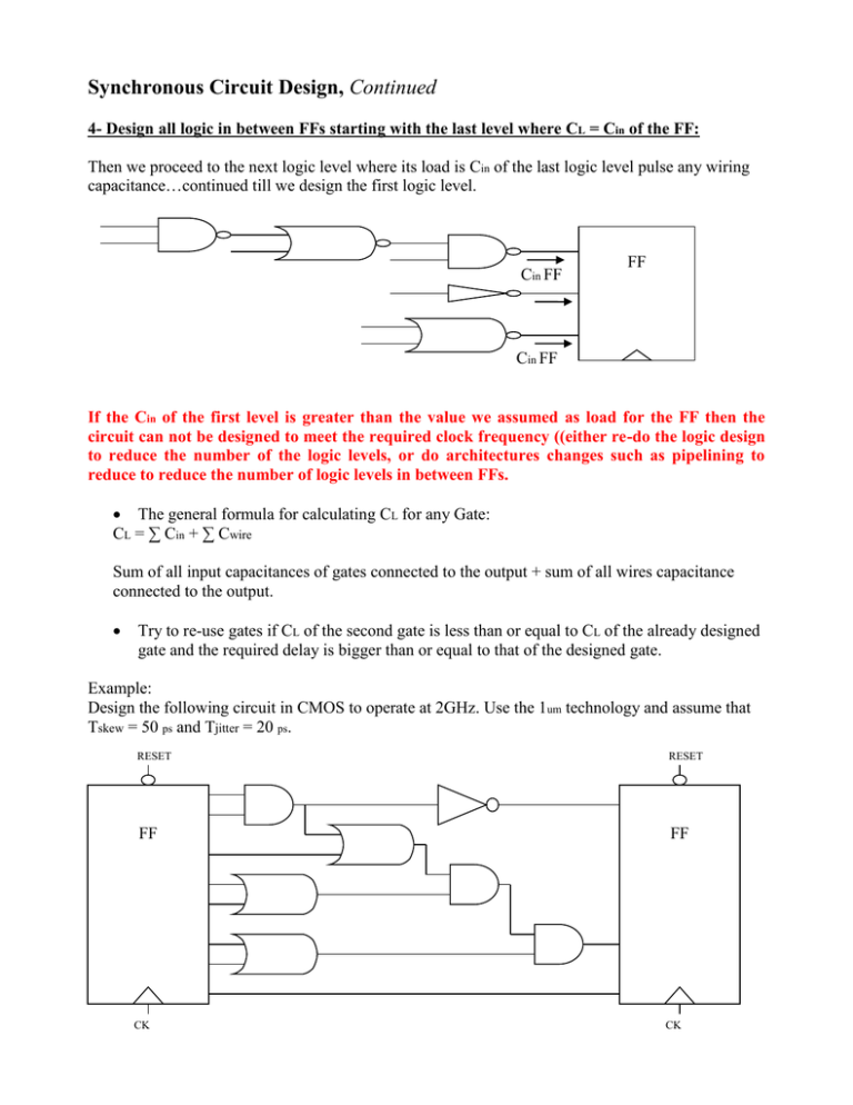
Synchronous Circuit Design, Continued 4- Design all logic in between FFs starting with the last level where CL = Cin of the FF: Then we proceed to the next logic level where its load is Cin of the last logic level pulse any wiring capacitance…continued till we design the first logic level. Cin FF FF Cin FF If the Cin of the first level is greater than the value we assumed as load for the FF then the circuit can not be designed to meet the required clock frequency ((either re-do the logic design to reduce the number of the logic levels, or do architectures changes such as pipelining to reduce to reduce the number of logic levels in between FFs. The general formula for calculating CL for any Gate: CL = ∑ Cin + ∑ Cwire Sum of all input capacitances of gates connected to the output + sum of all wires capacitance connected to the output. Try to re-use gates if CL of the second gate is less than or equal to CL of the already designed gate and the required delay is bigger than or equal to that of the designed gate. Example: Design the following circuit in CMOS to operate at 2GHz. Use the 1um technology and assume that Tskew = 50 ps and Tjitter = 20 ps. RESET RESET FF FF CK CK Sol: Try to combine groups (or clusters) of gates into single gates: RESET RESET FF FF CK CK Then convert to CMOS (insert bubbles): RESET RESET FF FF CK CK RESET RESET FF FF AOI 222 CK CK Total number of logic levels, including the FF = 2 + 4 = 6 TCK = 1/2GHz = 500 ps Delay per logic level = TCK – Tskew – Tjitter total number of logic = (500 – 50 – 20) / 6 ≈71 ps RESET 71 ps 71 ps RESET FF FF AOI 222 CK Required TSU2 = 2 X 71 = 142 ps CK and required TCKq1 = 2 X 71 = 142 ps Start by designing the FF assuming 50 fF load: Minimum size RESET RESET TG2 CK TG1 CK D 50fF CK CK CK CK Minimum size VDD SLAVE logic TD = 71 ps WPeff = 2 WNeff WNeff = WN WP WPeff = Wp/2 WP WP = 4 WN WN 50fF WN RN = TD/ CL = 71ps/50fF = 1.4 KΩ = (VDD – Vtn)/ (2IDsat/um *WNeff) -6 WNeff = 4.2/(2X500X10 X1.4X10³) = 2.8 um = WN WP = 4 WN = 11.2 um Cin = 2fF X1 (2.8 + 11.2) = 28fF RN WP This is CL for TG1: ≡ To design TG1: Let WP = 2 WN RN = RP TD = (RN /2) * CL WN RP RN = 2X71 /28fF ≈5KΩ -6 WN = 4.2/(1000X10 X5X10³ )≈ 0.8 um let WN = 1 um and WP = 2 um Then the MASTER logic VDD WNeff = WN /2 WPeff = WP Let WNeff = WPeff W P = WN WP WP 28fF RN = TD/ CL = 71ps/ 28fF = 2.5KΩ WN -6 WNeff = 4.2 / (1000X10 X2.5X10³) ≈1.6 um WN = 2X1.6 = 3.2 = WP Cin = 2fF X 1 (3.2+3.2) = 12.8fF WN This is also Cin of the FF WP = 2WN RN = 2TD Cin of the MASTER logic = 142ps / 12.8fF ≈ 11KΩ -6 WN = 4.2 / (1000X10 X11X 10³) = 0.4 um Let WN =1 um and WP =2 um FF is Done, We do the logic next
