302f0_05.doc
advertisement
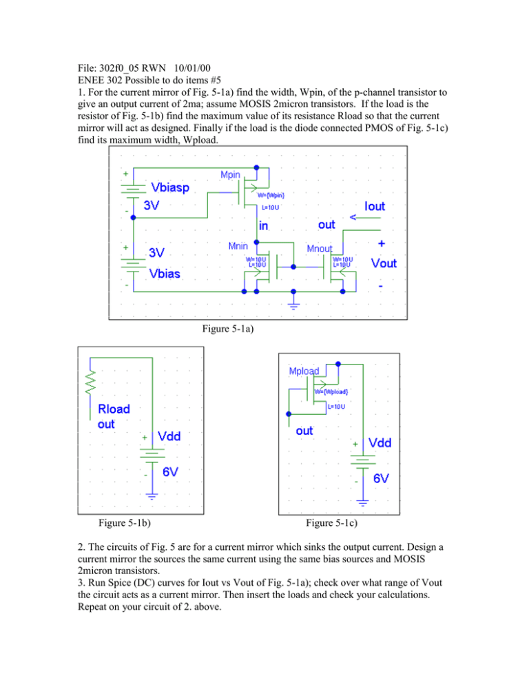
File: 302f0_05 RWN 10/01/00 ENEE 302 Possible to do items #5 1. For the current mirror of Fig. 5-1a) find the width, Wpin, of the p-channel transistor to give an output current of 2ma; assume MOSIS 2micron transistors. If the load is the resistor of Fig. 5-1b) find the maximum value of its resistance Rload so that the current mirror will act as designed. Finally if the load is the diode connected PMOS of Fig. 5-1c) find its maximum width, Wpload. Figure 5-1a) Figure 5-1b) Figure 5-1c) 2. The circuits of Fig. 5 are for a current mirror which sinks the output current. Design a current mirror the sources the same current using the same bias sources and MOSIS 2micron transistors. 3. Run Spice (DC) curves for Iout vs Vout of Fig. 5-1a); check over what range of Vout the circuit acts as a current mirror. Then insert the loads and check your calculations. Repeat on your circuit of 2. above.
