ENEE312H Spring 2002 Homework 6
advertisement

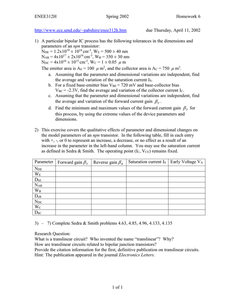
ENEE312H Spring 2002 http://www.ece.umd.edu/~pabshire/enee312h.htm Homework 6 due Thursday, April 11, 2002 1) A particular bipolar IC process has the following tolerances in the dimensions and parameters of an npn transistor: NDE = 1.2x10¹⁹ ± 1018 cm-3, WE = 500 ± 40 nm NAB = 4x10¹⁷ ± 2x1016 cm-3, WB = 350 ± 30 nm NDC = 4x10¹⁶ ± 1015 cm-3, WC = 1 ± 0.05 m The emitter area is AE = 100 m2, and the collector area is AC = 750 m2. a. Assuming that the parameter and dimensional variations are independent, find the average and variation of the saturation current IS. b. For a fixed base-emitter bias VBE = 720 mV and base-collector bias VBC = -2.3V, find the average and variation of the collector current IC. c. Assuming that the parameter and dimensional variations are independent, find the average and variation of the forward current gain F . d. Find the minimum and maximum values of the forward current gain F for this process, by using the extreme values of the device parameters and dimensions. 2) This exercise covers the qualitative effects of parameter and dimensional changes on the model parameters of an npn transistor. In the following table, fill in each entry with +, -, or 0 to represent an increase, a decrease, or no effect as a result of an increase in the parameter in the left-hand column. You may use the saturation current as defined in Sedra & Smith. The operating point (IC, VCE) remains fixed. Parameter Forward gain F NDE WE DhE NAB WB DeB NDC WC DhC Reverse gain R Saturation current IS Early Voltage VA 3) – 7) Complete Sedra & Smith problems 4.63, 4.85, 4.96, 4.133, 4.135 Research Question: What is a translinear circuit? Who invented the name “translinear”? Why? How are translinear circuits related to bipolar junction transistors? Provide the citation information for the first, definitive publication on translinear circuits. Hint: The publication appeared in the journal Electronics Letters. 1 of 1


