Proposal of a physics-based compact model for drift-di usion to ballistic transport
advertisement

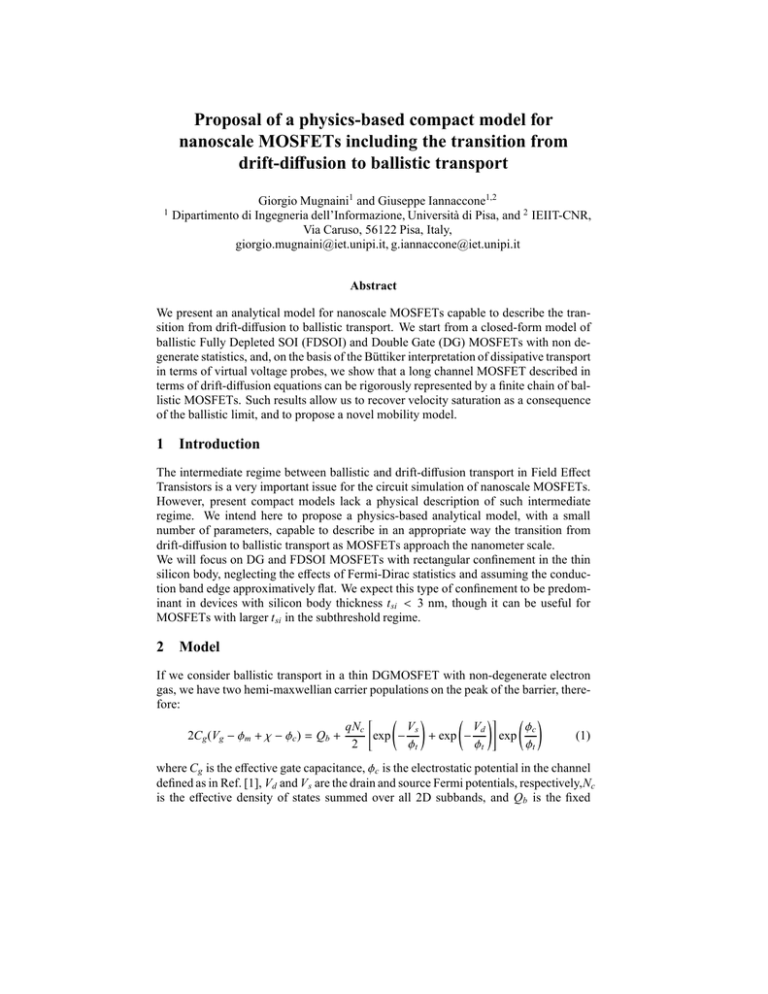
Proposal of a physics-based compact model for nanoscale MOSFETs including the transition from drift-diffusion to ballistic transport 1 Giorgio Mugnaini1 and Giuseppe Iannaccone1,2 Dipartimento di Ingegneria dell’Informazione, Università di Pisa, and 2 IEIIT-CNR, Via Caruso, 56122 Pisa, Italy, giorgio.mugnaini@iet.unipi.it, g.iannaccone@iet.unipi.it Abstract We present an analytical model for nanoscale MOSFETs capable to describe the transition from drift-diffusion to ballistic transport. We start from a closed-form model of ballistic Fully Depleted SOI (FDSOI) and Double Gate (DG) MOSFETs with non degenerate statistics, and, on the basis of the Büttiker interpretation of dissipative transport in terms of virtual voltage probes, we show that a long channel MOSFET described in terms of drift-diffusion equations can be rigorously represented by a finite chain of ballistic MOSFETs. Such results allow us to recover velocity saturation as a consequence of the ballistic limit, and to propose a novel mobility model. 1 Introduction The intermediate regime between ballistic and drift-diffusion transport in Field Effect Transistors is a very important issue for the circuit simulation of nanoscale MOSFETs. However, present compact models lack a physical description of such intermediate regime. We intend here to propose a physics-based analytical model, with a small number of parameters, capable to describe in an appropriate way the transition from drift-diffusion to ballistic transport as MOSFETs approach the nanometer scale. We will focus on DG and FDSOI MOSFETs with rectangular confinement in the thin silicon body, neglecting the effects of Fermi-Dirac statistics and assuming the conduction band edge approximatively flat. We expect this type of confinement to be predominant in devices with silicon body thickness t si < 3 nm, though it can be useful for MOSFETs with larger t si in the subthreshold regime. 2 Model If we consider ballistic transport in a thin DGMOSFET with non-degenerate electron gas, we have two hemi-maxwellian carrier populations on the peak of the barrier, therefore: " ! !# ! qNc φc Vs Vd 2Cg (Vg − φm + χ − φc ) = Qb + exp − + exp − exp (1) 2 φt φt φt where Cg is the effective gate capacitance, φc is the electrostatic potential in the channel defined as in Ref. [1], Vd and V s are the drain and source Fermi potentials, respectively,Nc is the effective density of states summed over all 2D subbands, and Qb is the fixed Equivalent Ballistic mobility Caughey-Thomas with n=2 Caughey-Thomas with n=1 Normalized Mobility µ/µ0 1 0.9 0.8 0.7 0.6 0.5 0.4 0.3 0.2 0.1 a) PSfrag replaements Vs N Vg 1 B B 1 2 3 4 Normalized Field E||/Ec 5 Vs b) B B Vd Vg Termalization 0 1 DD N 1 B 1 Vd Figure 1: a) Comparison of ballistic chain mobility with the Caughey-Thomas models for electrons and holes. b) Approximate aggregation of first N − 1 ballistic transistors in an equivalent Drift-Diffusion. The global circuit can be seen as a macromodel for a device in intermediate transport. charge per unit area in the body. This equation can be solved in terms of the Lambert W-function [2], and the current Ids is described by the following expression, that represents one of major results of the present paper: Vg −Vs −VT V −V −V ! e φt + e g φdt T + − vt tanh Vds Ids = I − I = Qn W (2) 2 2φt Remarkably, the previous description can also be used in the case of local equilibrium transport, i.e. drift-diffusion transport. Indeed, if we place V s = Vd = VFn where VFn is the local quasi Fermi potential we obtain the non-degenerate form of local vertical electrostatics proposed in [1]. We find for the mobile charge per unit area in local equilibrium Qm (VFn ): Vg − VT − VFn = Qm Qm + φt log 2Cg qNc (3) that is the same equation used in the EKV [3] model. Following the approach of Büttiker probes [4], a drift-diffusion MOSFET can be interpreted as a sufficiently long chain of ballistic transistors. We define Vk the Fermi potential at the k-th contact, and we assume that the k-th contact is placed at xk = kλ [x = 0 (x = L) corresponds to the source (drain)]. If N is the number of MOSFETs in the chain, current continuity enforced on the ballistic chain imposes N equations, corresponding to writing (2) for each ballistic MOSFET of the chain. If a voltage Vds is applied to the chain, we expect that each ballistic MOSFET is in the linear region if Vds /N << 2φt (no high field effects). If N is large enough, we can substitute the discrete Vk ’s with a continuous quasi-Fermi potential VFn , so that the ballistic equation (2) becomes: Ids = µn Qm ∇VFn , λvt that describes drift-diffusion transport with a low field mobility: µno ≡ 2φ , where λ is t the mean free path. If we integrate such equation along the channel, the current of a DD MOSFET is given by: µn Qn φt Q2ms − Q2md Qms − Qmd + Id = (4) , L Qn 2Q2n Vgs-VT=0.8V .4 2500 Vgs-VT=0.6V .3 1500 1000 .1 0 1 2 3 4 5 6 2DD*+B 3B 2DD+B 1B 2000 Vgs-VT=0.4V Vgs-VT=0.2V .2 0 a) 3000 Drain Current Ids[A/m] Fermi Level VFn[V] .5 7 8 Normalized abscissa x/L 9 10 500 00 b) 0.05 0.1 0.15 0.2 0.25 0.3 Drain Voltage Vds[V] Figure 2: a) Discrete quasi-Fermi potential with N = 10 at fixed Vds = 0.5V b) Output characteristics of different approximations. 2DD + 1B denotes the series of a driftdiffusion with L/λ = 2 and a ballistic transistor, 3DD denotes a drift-diffusion transistor with L/λ = 3, 2DD∗ + 1B denotes reduced mobility model [2]. tox = 2.5 nm. where Qms (Qmd ) is Qm computed at the source (drain), and Qn is the normalization charge 2Cg φt . Equation (4) constitutes the basic structure of EKV-like compact models [3].When the channel bias of each elementary transistor is larger than φt , limitation of the maximum current due to ballistic injection at each elementary source results in an effective reduction of the mobility µn . Mobility µn is defined as µn = vt tanh 2φλ t dVdxFn / dVdxFn , where the term 2φλ t can be interpreted as a “critical field ”, analogous to critical field in the saturation velocity effect. Such phenomenon exhibits a striking similarity with the Caughey-Thomas model for saturation velocity effect, as shown in Figure 1(a). We want to underline that a similar mobility expression was independently proposed by V.Arora in [5]. In order to build a more compact macromodel, we observe in the example in Fig.2(a), that when non-linear transport emerges, it manifests its effects approximatively only on the last ballistic transistor of the chain. This fact suggests that we can aggregate the first N − 1 ballistic transistors in an approximate equivalent drift-diffusion transistor with ratio L/λ = N − 1, as schematically represented in Fig.1(b). In Figure 2(b) the output characteristics of a series of N = 3 ballistic transistors and possible macromodels are compared: the series of one DD and one ballistic transistor has a small but not negligible error. The reason of such error is the approximation of linear transport in the first N − 1 transistors. However, it is possible to improve the approximation in the simple way discussed in [2], leading to the line denoted by “DD∗ + B”. An important point is that no smoothed clamp to an “effective Vds ” has been used, because its role is covered by the ballistic MOSFET. In order to describe the 2D electrostatic effects we introduce two geometrical capacitances C s , Cd that model coupling to the source and drain, responsible for DIBL. Degradation of mobility at high vertical fields, series resistances and polysilicon depletion effect are introduced in the model [2] and are described by four additional parameters: R s , Rd , N p , θ. In Figure 3 the characteristics obtained from our proposed model and experimental data for a FinFET with channel length L = 80 nm from Ref. [6]. The proposed model is not yet complete, but we believe that the proposed interpretation can be the basis of more physical compact models. 1000 1000 Compact model Experimental [6] 100 Ids[A/m] Ids[A/m] 800 600 400 10 1 200 0 Compact Model Experimental [6] 0 0.2 0.4 0.6 0.8 Vds[V] 1 1.2 0.1 -0.5 0 0.5 Vgs[V] 1 Figure 3: Output (left) and transfer (right) characteristics of a FinFET with L = 80 nm: experiments (solid line) and proposed model (squares). 3 Conclusions We have proposed a novel closed-form solution for ballistic ultrathin body MOSFET. Our model is analytical, explicit and inherently symmetrical. We have shown that a long chain of ballistic MOSFETs can be interpreted as a drift-diffusion transistor with constant mobility, while if the device is shorter, a behavior emerges similar to the saturation velocity effect. Then, we have proposed a physics-based macromodel for short MOSFETs is proposed. Because of its structure, this model can be thought as a generalization of EKV-like models [3] such as ACM, USIM, and it is suitable for circuit simulation. We anticipate an extension to Fermi-Dirac statistics [2] that describes a mobility degradation caused by degeneracy. Support from Fondazione Cassa di Risparmio di Pisa and from the EU through the NoE SINANO is gratefully acknowledged. References [1] G. Baccarani and S. Reggiani,”A compact double-gate MOSFET model comprising quantum-mechanical and nonstatic effects”, IEEE Trans. Electron Devices, vol. 46, pp. 16561666, Aug. 1999. [2] G. Mugnaini and G. Iannaccone, ”Physics-based compact models of nanoscale MOSFETs : Transition from drift-diffusion to ballistic transport”, unpublished, 2004. [3] C.C.Enz, F.Krummenacher and E.Vittoz, ”An analytical MOS transistor model valid in all regions of operation and dedicated to low-voltage and low-power applications”, Analog Integ. Circuits Signal Proc, 1995. [4] M.Büttiker, ”Role of quantum coherence in series resistors”, Phys. Rev. B, no. 33, pp. 30203026, 1986. [5] V. K. Arora, ”Drift diffusion and Einstein relation for electrons in silicon sujected to a high electric field”, Applied Physics Letters, vol. 80, no. 20, pp. 3763-3765, May 2002. [6] B. Yu, L. Chang, S. Ahmed, H. Wang, S. Bell, C.-Y. Yang, C. Tabery, C. Ho, Q. Xiang, T.-J. King, J. Bokor, C. Hu, M.-R. Lin, and D. Kyser, ”FinFET scaling to 10 nm gate length”, in IEDM Digest International 2002, Dec. 2002.


