APEX II Clock-Data Synchronization (CDS)
Competitive Advantage
Technical Brief 78
January 2002, ver. 1.1
Introduction
Altera Corporation
101 Innovation Drive
San Jose, CA 95134
(408) 544-7000
http://www.altera.com
http://www.altera.com/mysupport
With the expansion of the Internet and telecommunications markets, designers face the
challenge of providing higher bandwidth systems and higher performance. Many designers
use differential signaling and source-synchronous clocking to deliver the required
performance. Although these techniques address signal integrity and data-transfer rate
requirements, source-synchronous clocking is inflexible, and clock-to-data skew remains a
problem to be solved.
The data-transfer rate increase imposes a stringent timing budget for designers using
source-synchronous clocking. In addition to the timing variation during system operation,
other problems can cause a system to malfunction. Example problems are threshold and
delay mismatch of driver output cells, edge-rate mismatch between clock-and-data output
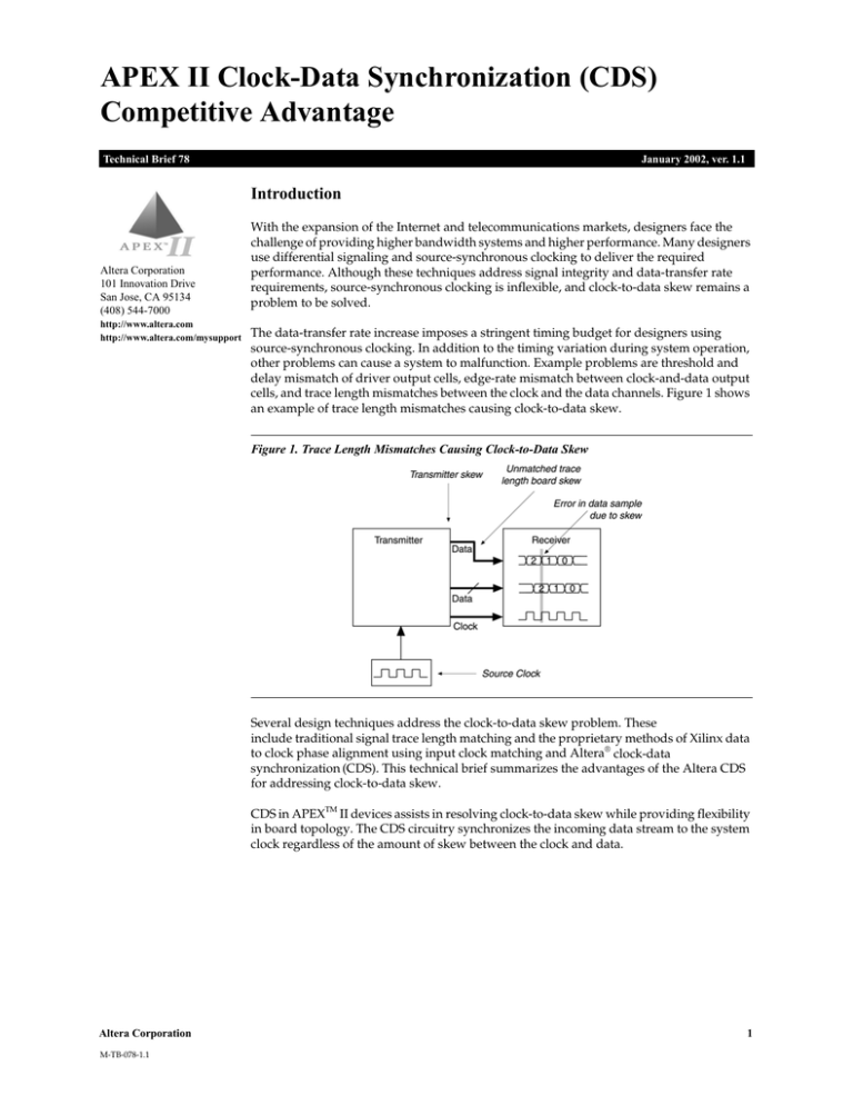
cells, and trace length mismatches between the clock and the data channels. Figure 1 shows
an example of trace length mismatches causing clock-to-data skew.
Figure 1. Trace Length Mismatches Causing Clock-to-Data Skew
Several design techniques address the clock-to-data skew problem. These
include traditional signal trace length matching and the proprietary methods of Xilinx data
to clock phase alignment using input clock matching and Altera® clock-data
synchronization (CDS). This technical brief summarizes the advantages of the Altera CDS
for addressing clock-to-data skew.
CDS in APEXTM II devices assists in resolving clock-to-data skew while providing flexibility
in board topology. The CDS circuitry synchronizes the incoming data stream to the system
clock regardless of the amount of skew between the clock and data.
Altera Corporation
M-TB-078-1.1
1
TB 78: APEX II Clock-Data Synchronization (CDS) Competitive Advantage
CDS Description
CDS dedicated circuitry in APEX II devices over-samples a predetermined training pattern
on the data channel to align the input system clock with the data stream. Depending on the
CDS operation mode, the internal over-sampling circuit provides either five or eight phaseshifted clock signals to capture the data in each channel. CDS circuitry operates in three
different modes: single-bit mode, multi-bit mode, and pre-programmed CDS mode. Each
mode provides a different level of clock-to-data skew tolerance.
■
■
■
Single-bit mode compensates for skew up to 50% of the data bit period and preserves
the byte alignment by using a predetermined training pattern. Figure 2 depicts the
operation of single-bit mode CDS.
Multi-bit mode compensates for unlimited clock-to-data skew using an alternating 0
and 1 training pattern. A byte alignment circuit is required.
Pre-programmed CDS compensates for clock-to-data skew up to 50% of the data bit
period while preserving byte alignment. It also compensates for unlimited skew with a
byte alignment circuit. A time domain reflectometry (TDR) measurement can
determine the amount of skew existing on the board. The designer pre-programs the
device to compensate for the measured skew.
Figure 2. Single-Bit CDS Operation Clock & Data Input
Without the convenience of CDS, designers must rely on signal trace length matching or
input clock phase-alignment methods to combat clock-to-data skew.
Trace Length Matching
Trace length matching is a technique that attempts to solve the clock-to-data skew problem
by manually maintaining equal trace length for each data channel and the clock. Previously
the standard technique, trace length matching was the only viable solution before the
introduction of CDS, and it has the following disadvantages:
■
■
■
2
It does not support flexible board topologies. The clock signal needs to be forwarded
from each of the transmitting devices even if they are all driven by the same clock. Each
transmitting device may introduce a new clock domain.
It requires significant engineering time to precisely match the clock signal and each
data channel trace length.
It is intolerant of temperature variations or other unexpected operational
environmental changes. The operation condition variation may change the amount of
skew between each signal trace.
Altera Corporation
TB 78: APEX II Clock-Data Synchronization (CDS) Competitive Advantage
Input Clock Matching
The Xilinx Virtex-E device's delay-locked loop (DLL) and Virtex-II device's digital clock
manager (DCM) attempt to resolve the clock-to-data skew by phase-shifting the input
system clock signal and by using the phase aligner circuit.
The input system clock is first processed by the DLL or DCM to generate two clock
outputs that are 90-degree phase-shifted. The phase aligner module samples the input
data stream using both the rising and falling edge of these two clocks. Flip flops in the
internal logic store the data samples. Then, one of the four data sample sets is selected
to be the valid input data.
Input clock matching has the following disadvantages:
■
■
■
■
It requires the trace length between each of the data channels to be exactly the same
so that channel-to-channel skew is identical.
It requires the addition of phase aligner modules, which consume internal logic
elements (LEs) — reducing the device capacity for system logic — to interface with
each input data bus.
It requires the clock to be forwarded from the transmitting device.
Its system speed is limited due to the limitation in producing both 0 and 90 degree
phase-shifted clocks using DLL and DCM. To produce the required phase-shifted
clocks, the input clock for the Virtex-E DLL is limited to a maximum of 160Mhz
while the Virtex-II DCM must run in low-frequency mode.
Advantages of CDS in APEX II Devices
CDS in APEX II devices, in addition to eliminating the clock-to-data skew issue,
provides significant advantages over other solutions.
■
■
■
■
■
■
■
■
Altera Corporation
Dedicated circuitry implements CDS to provide ease-of-use for the designer.
A system can use CDS to re-synchronize during run-time to account for skew
caused by clock drift or unexpected changes in operation condition.
The transmitting device does not have to forward the clock; rather, the clock signal
for the APEX II devices can be fed directly from the board clock source as shown
in Figure 3.
CDS provides flexibility in board topology.
APEX II True-LVDSTM circuitry supports up to two different clock domains to
further expand its flexibility to interface with multiple data sources.
CDS operates independently on each receiver channel and alleviates the need for
the designers to exactly match each of the on-board trace lengths (unlimited
channel-to-channel skew).
Multi-bit CDS can correct unlimited clock-to-data skew.
In single-bit or multi-bit mode, CDS does not require the knowledge of clock-todata skew prior to board design and fabrication.
3
TB 78: APEX II Clock-Data Synchronization (CDS) Competitive Advantage
Figure 3. Single-Clock Synchronous Topology
Table 1 compares APEX II CDS, trace length matching, and Xilinx Virtex-II/Virtex-E
input clock matching.
Table 1. Comparison of APEX II CDS to Other Solutions
Category
APEX II CDS
Trace Length Matching
Virtex-II/Virtex-E Input
Clock Matching
Clock-to-data skew elimination
v
v
v (requires trace length
matching & phase aligner)
Channel-to-channel skew elimination
v
v
Dynamic skew elimination
v
N:1 single-clock synchronous topology
v
Switch topology
v
Matrix topology
v
Multiple clock domain support
v
Ease of implementation
v
v
Conclusion
Systems requiring high-speed data transfer magnify the importance of clock-to-data
skew. The easy-to-use CDS feature in APEX II devices eliminates static board skew,
provides the capability to handle run-time skew, and allows flexibility in board
topology. Altera APEX II devices are the best solution for high-speed, high-bandwidth
system designs.
Altera Corporation
4
TB 78: APEX II Clock-Data Synchronization (CDS) Competitive Advantage
Reference
For detailed information about the APEX-II CDS feature and board topology, refer to
Application Note 157 (Using CDS in APEX II Devices) and Application Note 162 (Increasing
System Bandwidth with CDS).
®
101 Innovation Drive
San Jose, CA 95134
(408) 544-7000
http://www.altera.com
Altera Corporation
Copyright © 2002 Altera Corporation. All rights reserved. Altera, The Programmable Solutions Company, the stylized Altera logo, specific
device designations, and all other words and logos that are identified as trademarks and/or service marks are, unless noted otherwise, the
trademarks and service marks of Altera Corporation in the U.S. and other countries. All other product or service names are the property of
their respective holders. Altera products are protected under numerous U.S. and foreign patents and pending applications, maskwork rights,
and copyrights. Altera warrants performance of its semiconductor products to current specifications in accordance with Altera’s standard
warranty, but reserves the right to make changes to any products and services at any time without notice. Altera assumes no responsibility or
liability arising out of the application or use of any information, product, or service described herein except as expressly agreed to in writing
by Altera Corporation. Altera customers are advised to obtain the latest version of device specifications before relying on any published
information and before placing orders for products or services.
5
