FLEX PCI Development Kit
Solution Brief 46
December 1999, ver. 1
Target Applications:
Features
All PCI-based systems
■
Family:
FLEX® 10K
■
Ordering Code:
PCI-BOARD2
■
Vendor:
■
■
®
101 Innovation Drive
San Jose, CA 95134
http://www.altera.com
Tel. (408) 544-7000
■
■
32-bit to 64-bit/33-MHz to 66-MHz peripheral component interconnect (PCI)
development and prototyping platform
Easy-to-use Windows-based program for design analysis and system performance
measurement
Includes a demonstration design with the pci_mt64 MegaCoreTM function, an
SDRAM controller, a direct memory access (DMA) controller, a first-in first-out
(FIFO) buffer, and control logic
FLEX® 10KE EPF10K100E-1 device in a 484-pin FineLine BGATM package
On-board features:
– I/O prototype area for custom logic
– DB9 connector for RS-232 serial communication
– Standard PMC connector
– 144-pin small outline DIMM 32-Mbyte SDRAM module
– Voltage regulator that automatically generates 2.5 V and 3.3 V from a 5.0-V
power supply
Supports in-circuit reconfiguration with an EPC2 configuration device and a
ByteBlasterMVTM download cable
Flexible clocking options for on-board logic, including a PCI clock, an on-board
crystal oscillator, or an external clock
General Description
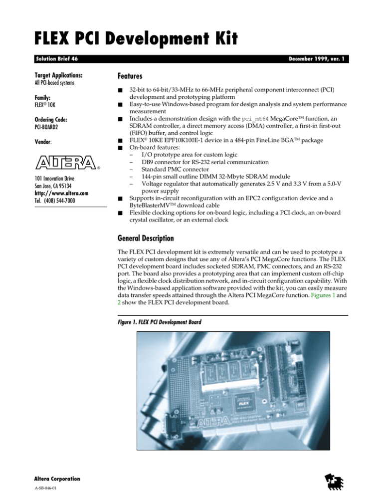
The FLEX PCI development kit is extremely versatile and can be used to prototype a
variety of custom designs that use any of Altera’s PCI MegaCore functions. The FLEX
PCI development board includes socketed SDRAM, PMC connectors, and an RS-232
port. The board also provides a prototyping area that can implement custom off-chip
logic, a flexible clock distribution network, and in-circuit configuration capability. With
the Windows-based application software provided with the kit, you can easily measure
data transfer speeds attained through the Altera PCI MegaCore function. Figures 1 and
2 show the FLEX PCI development board.
Figure 1. FLEX PCI Development Board
Altera Corporation
A-SB-046-01
ALTERA MEGAFUNCTION PARTNERS PROGRAM
SB 46: FLEX PCI Development Kit
Figure 2. FLEX PCI Development Board Schematic
Local-Side Clock Input
User Prototype Area
32-Byte SDRAM Module
+ C2
+ C4
U2
L2
+ C3
D2
U1
L1
D1
+ C1
+ C5
General Purpose
LEDs
JN2
LED1
JN1
C8 +
JP1
I/O 1-64
External Power
Input
+
PMC Connector
JP2
JN3
U4
PS Header
JN4
S2
JP3
C9
+
S1
SDRAM SOCKET
C10
Clock
+
RS-232
Header
C14
+
C11
JTAG Header
JP4
Oscillator
Dedicated
Input 1-3
+5.0 V
+3.3 V
+2.5 V
GND
Proto 1-20
Program Switch
+
U6
¤
U3
¤
U7
+
U8
+
U9
EPF10K100EFC484-1
U5
C12
¤
+
+
C6
C13
EPC2
U10
JP5
C15
P1
C7
Edge Connector
PCI Interface
FLEX PCI Development Kit Deliverables
Altera provides the following items with the FLEX PCI development kit:
■
■
■
■
FLEX PCI development board
ByteBlasterMV parallel port download cable
CD-ROM containing all PCI MegaCore functions, demonstration designs, and
support literature
Development board schematics are available upon request
®
101 Innovation Drive
San Jose, CA 95134
(408) 544-7000
http://www.altera.com
2
Copyright 1999 Altera Corporation. Altera, FLEX, FLEX 10K, FLEX 10KE, EPF10K100E, EPC2, FineLine BGA, MegaCore, and ByteBlasterMV
are trademarks and/or service marks of Altera Corporation in the United States and other countries. Other brands or products are trademarks
of their respective holders. The specifications contained herein are subject to change without notice. Altera assumes no responsibility or
liability arising out of the application or use of any information, product, or service described herein except as expressly agreed to in writing
by Altera Corporation. Altera customers are advised to obtain the latest version of device specifications before relying on any published
information and before placing orders for products or services. All rights reserved.
Altera Corporation


