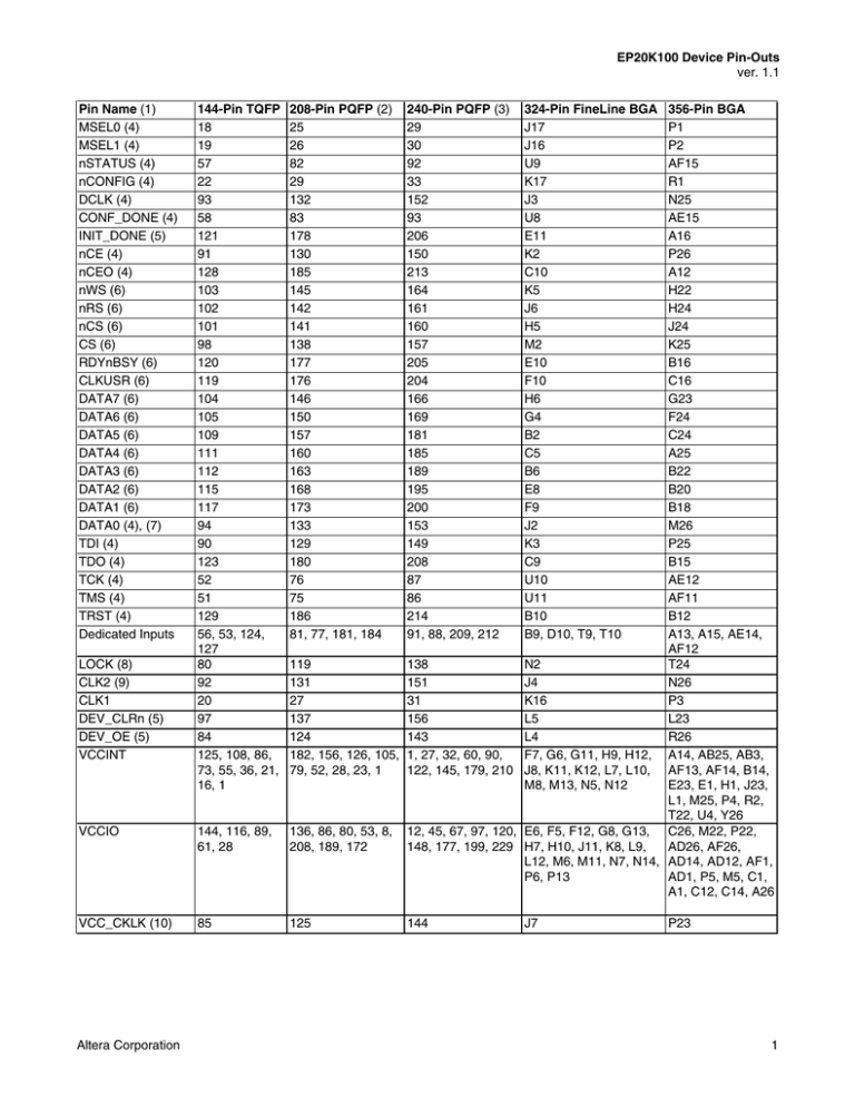
EP20K100 Device Pin-Outs
ver. 1.1
Pin Name (1)
MSEL0 (4)
MSEL1 (4)
nSTATUS (4)
nCONFIG (4)
DCLK (4)
CONF_DONE (4)
INIT_DONE (5)
nCE (4)
nCEO (4)
nWS (6)
nRS (6)
nCS (6)
CS (6)
RDYnBSY (6)
CLKUSR (6)
DATA7 (6)
DATA6 (6)
DATA5 (6)
DATA4 (6)
DATA3 (6)
DATA2 (6)
DATA1 (6)
DATA0 (4), (7)
TDI (4)
TDO (4)
TCK (4)
TMS (4)
TRST (4)
Dedicated Inputs
LOCK (8)
CLK2 (9)
CLK1
DEV_CLRn (5)
DEV_OE (5)
VCCINT
144-Pin TQFP
18
19
57
22
93
58
121
91
128
103
102
101
98
120
119
104
105
109
111
112
115
117
94
90
123
52
51
129
56, 53, 124,
127
80
92
20
97
84
125, 108, 86,
73, 55, 36, 21,
16, 1
VCCIO
144, 116, 89,
61, 28
VCC_CKLK (10)
85
Altera Corporation
208-Pin PQFP (2)
25
26
82
29
132
83
178
130
185
145
142
141
138
177
176
146
150
157
160
163
168
173
133
129
180
76
75
186
81, 77, 181, 184
240-Pin PQFP (3)
29
30
92
33
152
93
206
150
213
164
161
160
157
205
204
166
169
181
185
189
195
200
153
149
208
87
86
214
91, 88, 209, 212
324-Pin FineLine BGA
J17
J16
U9
K17
J3
U8
E11
K2
C10
K5
J6
H5
M2
E10
F10
H6
G4
B2
C5
B6
E8
F9
J2
K3
C9
U10
U11
B10
B9, D10, T9, T10
356-Pin BGA
P1
P2
AF15
R1
N25
AE15
A16
P26
A12
H22
H24
J24
K25
B16
C16
G23
F24
C24
A25
B22
B20
B18
M26
P25
B15
AE12
AF11
B12
A13, A15, AE14,
AF12
119
138
N2
T24
131
151
J4
N26
27
31
K16
P3
137
156
L5
L23
124
143
L4
R26
182, 156, 126, 105, 1, 27, 32, 60, 90,
F7, G6, G11, H9, H12, A14, AB25, AB3,
79, 52, 28, 23, 1
122, 145, 179, 210 J8, K11, K12, L7, L10, AF13, AF14, B14,
E23, E1, H1, J23,
M8, M13, N5, N12
L1, M25, P4, R2,
T22, U4, Y26
136, 86, 80, 53, 8, 12, 45, 67, 97, 120, E6, F5, F12, G8, G13, C26, M22, P22,
AD26, AF26,
208, 189, 172
148, 177, 199, 229 H7, H10, J11, K8, L9,
L12, M6, M11, N7, N14, AD14, AD12, AF1,
P6, P13
AD1, P5, M5, C1,
A1, C12, C14, A26
125
144
J7
P23
1
EP20K100 Device Pin-Outs
ver. 1.1
Pin Name (1)
GNDINT
144-Pin TQFP 208-Pin PQFP (2) 240-Pin PQFP (3)
126, 87, 77,
183, 143, 127, 118, 19, 28, 42, 89, 137,
74, 54, 34, 17, 78, 39, 24, 16
146, 162, 211
4
GNDIO (11)
134, 106, 72,
42, 12
GND_CKLK (10)
No Connect (N.C.)
88
–
Total User I/O Pins 101
(12)
Altera Corporation
324-Pin FineLine BGA
G9, D4, D15, E5, E14,
F6, F13, G7, G12, H8,
H11, J9, J10, K9, K10,
L8, L11, M7, M12, N6,
N13, P5, P14, R4, R15
356-Pin BGA
AB4, AB5, AC3,
AC22, AC23,
AC24, AD2, AD13,
AD25, AE1, AE13,
AE26, B1, B13,
B26, C2, C13,
C25, D3, D4, D22,
D23, D24, E5, N3,
N4, N5, N22, N23,
N24
199, 169, 149, 114, 26, 56, 78, 108,
–
95, 64, 43, 10
132, 165, 188, 218,
240
128
147
K7
–
–
–
–
159
252
189
252
P24
AA26, AA25, AA3,
AA2, AA1, AA24,
AA23, AB26, AB2,
AB1, AB24, AB23,
AB22, AC26,
AC25, AC2, AC1,
D2, D1, E4, E3,
E2, J25, K26, K23
2
EP20K100 Device Pin-Outs
ver. 1.1
Notes:
(1) All pins that are not listed are user I/O pins.
(2) EP20K100 devices in 208-pin PQFP packages are pin-compatible with EP20K200 devices in the same
package if pins 154, 148, 121, 109, 48, 36, 11, and 3 are tri-stated and connected to VCCINT, and if
pins 153, 147, 110, 47, 35, 12, and 4 are tristated and connected to GNDINT.
(3) EP20K100 devices in 240-pin PQFP packages are pin-compatible with EP20K200 devices in the same
package if pins 176, 168, 140, 127, 52, 39, 14, and 5 are tri-stated and connected to VCCINT, and if
pins 175, 167, 128, 51, 38, 15, and 6 are tri-stated and connected to GNDINT.
(4) This pin is a dedicated pin; it is not available as a user I/O pin.
(5) This pin can be used as a user I/O pin if it is not used for its device-wide or configuration function.
(6) This pin can be used as a user I/O pin after configuration.
(7) This pin is tri-stated in user mode.
(8) This pin shows the status of the ClockLock and ClockBoost circuitry. When the ClockLock and
ClockBoost circuitry is locked to the incoming clock and generates an internal clock, LOCK is driven
high. LOCK remains high if a periodic clock stops clocking. The LOCK function is optional; if the LOCK
output is not used, this pin is a user I/O pin.
(9) This pin drives the ClockLock and ClockBoost circuitry.
(10) This pin is the power or ground for the ClockLock and ClockBoost circuitry. To ensure noise resistance,
the power and ground supply to the ClockLock and ClockBoost circuitry should be isolated from the
power and ground to the rest of the device. VCC_CKLK has the same voltage specifications as the
VCCINT and should be connected to a 2.5-V power supply. If the ClockLock or ClockBoost circuitry is
not used, this power or ground pin should be connected to VCCINT or GNDINT, respectively.
(11) GNDIO and GNDINT are connected together in BGA packages.
(12) The user I/O pin count includes dedicated inputs, dedicated clock inputs, and all I/O pins.
Altera Corporation
3
Copyright © 1995, 1996, 1997, 1998, 1999 Altera Corporation, 101 Innovation Drive,
San Jose, CA 95134, USA, all rights reserved.
By accessing this information, you agree to be bound by the terms of Altera’s
Legal Notice.
