Implementing SFI-4 in
Stratix Devices
March 2002, ver. 1.0
Introduction
Application Note 219
The growth of the Internet has created huge bandwidth demands as voice,
video, and data push the limits of the existing wide area network (WAN)
backbones. To facilitate this bandwidth growth, speeds of OC-192 and
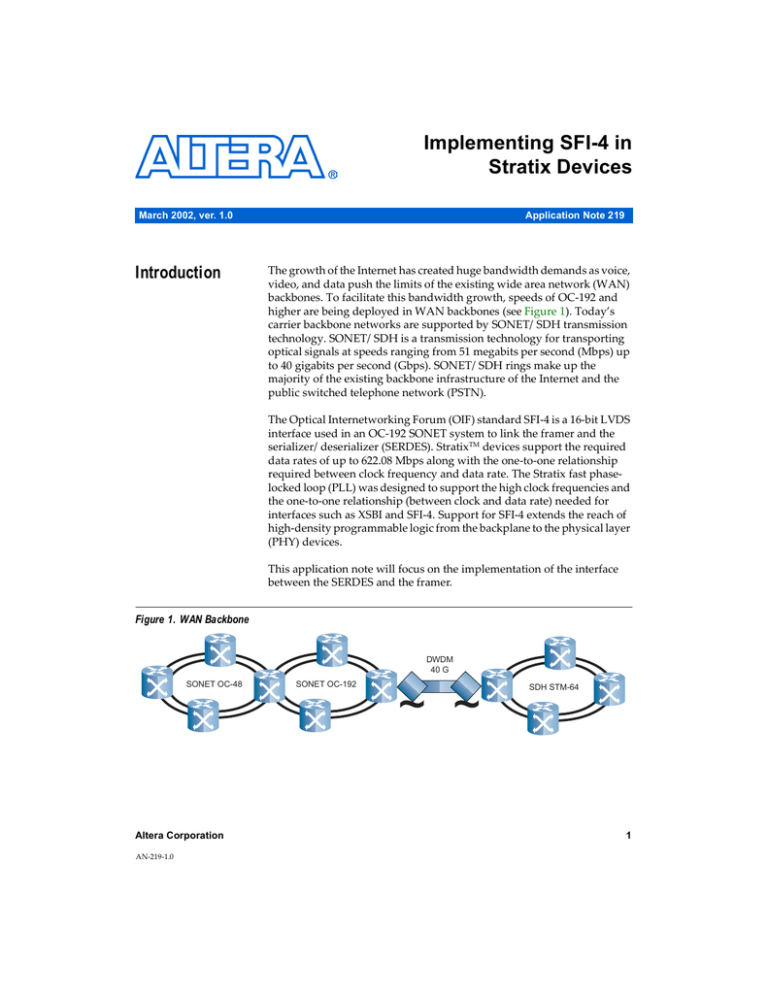
higher are being deployed in WAN backbones (see Figure 1). Today’s
carrier backbone networks are supported by SONET/SDH transmission
technology. SONET/SDH is a transmission technology for transporting
optical signals at speeds ranging from 51 megabits per second (Mbps) up
to 40 gigabits per second (Gbps). SONET/SDH rings make up the
majority of the existing backbone infrastructure of the Internet and the
public switched telephone network (PSTN).
The Optical Internetworking Forum (OIF) standard SFI-4 is a 16-bit LVDS
interface used in an OC-192 SONET system to link the framer and the
serializer/deserializer (SERDES). StratixTM devices support the required
data rates of up to 622.08 Mbps along with the one-to-one relationship
required between clock frequency and data rate. The Stratix fast phaselocked loop (PLL) was designed to support the high clock frequencies and
the one-to-one relationship (between clock and data rate) needed for
interfaces such as XSBI and SFI-4. Support for SFI-4 extends the reach of
high-density programmable logic from the backplane to the physical layer
(PHY) devices.
This application note will focus on the implementation of the interface
between the SERDES and the framer.
Figure 1. WAN Backbone
DWDM
40 G
SONET OC-48
Altera Corporation
AN-219-1.0
SONET OC-192
~ ~
SDH STM-64
1
AN 219: Implementing SFI-4 in Stratix Devices
A SONET/SDH transmission network is composed of several pieces of
equipment, including terminal multiplexers, add-drop multiplexers, and
repeater and digital cross-connect systems. SONET is the standard used
in North America and SDH is the standard used outside North America.
The SONET/SDH specification outlines the frame format, multiplexing
method, synchronization method, and optical interface between the
equipment, as well as the specific optical interface.
SONET/SDH continues to play a key role in the next generation of
networks for many carriers. In the core network, the carriers offer services
such as telephone, dedicated leased lines, and Internet protocol (IP) data,
which are continuously transmitted. The individual data channels are not
transmitted on separate lines; instead, they are multiplexed into higher
speeds and transmitted on SONET/SDH networks at the corresponding
transmission speed.
Figure 2 shows a typical SONET/SDH line card. The system operates as
follows:
2
1.
The SONET/SDH line card first takes a high-speed serial optical
signal and converts it into a high-speed serial electrical signal. The
devices are called physical media dependent (PMD) devices.
2.
The system then recovers the clock from the electrical data using a
clock data recovery (CDR) unit.
3.
The SERDES parallelizes the data so that it can be manipulated
easily at lower clock rates.
4.
The interface between the SERDES and framer is called the SERDES
framer interface. The interface requirements are defined by the OIF.
5.
The framer identifies the beginning of the SONET/SDH frames and
monitors the performance of the system.
6.
The mapper following the framer maps asynchronous transfer mode
(ATM) cells, IP packets, or T/E carrier signals into the SONET frame.
7.
The PHY-link layer interface provides a bus interface to packet/cell
processors or other link-layer devices.
Altera Corporation
AN 219: Implementing SFI-4 in Stratix Devices
Figure 2. SONET/SDH Line Card
7
1
Optical
Signal
OE Module
2
CDR
3
5
6
SERDES
SONET/SDH
Framer
SONET/SDH
Mapper/Protocol
Processor
Optical-Electrical
Conversion
SERDES Framer
Interface
4
To Packet
Processor &
Switch Fabric
Link Layer
Interface
The OIF has defined the electrical interface (SFI) between the
SONET/SDH framer and high-speed SERDES devices. To keep up with
evolving transmission speeds and technology enhancements, different
versions of electrical interfaces are defined. SFI-4 is the version of SFI that
acts as an interface between an OC-192 SERDES and SONET framer, as
shown in Figure 2. An aggregate of 9953.28 Mbps is transferred in each
direction. With their differential I/O capabilities, Stratix devices are
ideally suited to support the framer side of the SFI-4 interface. Support for
SFI-4 extends the reach of high-density programmable logic from the
backplane to the PHY devices.
System Topology
The SFI-4 interface uses 16 channels of source-synchronous LVDS to
interface between a SONET framer and an OC-192 SERDES. Figure 3
shows the SFI-4 interface.
Altera Corporation
3
AN 219: Implementing SFI-4 in Stratix Devices
Figure 3. SFI-4 Interface Signals
REFCLK
SONET Framer
Transmitter
OC-192 SERDES
Transmitter
TXDATA[15..0]
TXCLK
TXCLK_SRC
SONET Framer
Receiver
Recovered Clock
Receiver
RXDATA[15..0]
RXCLK
The framer transmits outbound data via TXDATA[15..0] and is received
at the SERDES using TXCLK. TXCLK is derived from TXCLK_SRC, which
is provided by the OC-192 SERDES. The framer receives incoming data on
RXDATA[15..0] from the OC-192 SERDES. The data received is latched
on the rising edge of RXCLK. Table 1 provides the data rates and clock
frequencies specified by SFI-4. The modes of TXCLK are specified by the
SFI-4 standard. In required mode (622 MHz clock mode or ×1 mode),
TXCLK should run at 622.08 MHz. In optional mode (311 MHz clock mode
or ×2 mode), TXCLK should run at 311.04 MHz.
Table 1. SFI-4 Interface Data Rates & Clock Frequencies
Signal
TXDATA[15..0]
TXCLK
4
Performance
622.08 Mbps
622.08 MHz or 311.04 MHz
TXCLK_SRC
622.08 MHz
RXDATA[15..0]
622.08 Mbps
RXCLK
622.08 MHz
REFCLK
622.08 MHz
Altera Corporation
AN 219: Implementing SFI-4 in Stratix Devices
Interface Implementation in Stratix Devices
The 16-bit full-duplex LVDS implementation of the framer part of the
SFI-4 interface is shown in Figure 4. Stratix devices support sourcesynchronous interfacing and LVDS differential signaling up to 840 Mbps.
Stratix devices have embedded SERDES circuitry for serial and parallel
data conversion. The Stratix fast PLL enables 622.08 Mbps data
transmission by transmitting and receiving a differential clock at rates of
up to 645 MHz. The clocks required in the SERDES for parallel and serial
data conversion can be configured from the received RXCLK (divided
down), the TXCLK_SRC (divided down), or the asynchronous core clock.
See Figure 4.
Figure 4. Implementation of SFI-4 Interface Using Stratix Devices
REFCLK
OC-192
SERDES
128
Data
TXDATA[15..0]
Transmitter
SERDES
Clk
TXCLK
Stratix Framer
PLL1
Stratix
Logic
Array
×1
TXCLK_SRC
÷8
Transmitter
Transmitter
Receiver
PLL2
Phase Shift
÷8
Clk
180˚
Receiver
SERDES
RXCLK
RXDATA[15..0]
Data
128
Receiver
f
Altera Corporation
For details on differential I/O buffers, SERDES, and clock dividers using
PLLs, refer to AN 202: Using High-Speed Differential I/O Interfaces in Stratix
Devices.
5
AN 219: Implementing SFI-4 in Stratix Devices
Figure 5 shows the transmitter block (from Figure 4) of the SFI-4 framer
interface implemented in Stratix devices. The data starts in the logic array
and goes into the Stratix SERDES block. The transmitter SERDES of the
framer converts the parallel data to serial data for the 16 TXDATA channels
(TXDATA[15..0]). A fast PLL is used to generate TXCLK from
TXCLK_SRC. The fast PLL keeps the TXDATA and TXCLK edge-aligned. A
divided down (÷8) clock generated from TXCLK_SRC is used to convert
the parallel data to serial in the transmitter SERDES. The divided down
clock also clocks some of the logic in the logic array.
Figure 5. Framer Transmitter Interface in Stratix Devices
Stratix SFI-4 Transmitter
Stratix SERDES
Parallel
Register
8
Parallel-to-Serial
Register
CH0
TXDATA[0]
622 Mbps
Stratix Logic
Array
OC-192
SERDES
8
CH15
TXDATA[15]
TXCLK
622MHz
÷J
Fast PLL
×W
622 MHz
W=1
J=8
TXCLK_SRC
622 MHz
Figure 6 shows the receiver block (from Figure 4) of the SFI-4 framer
interface implemented in Stratix devices. RXDATA[15..0] is received
from the OC-192 SERDES on the differential I/O pins of the Stratix device.
The receiver SERDES converts the high-speed serial data to parallel. You
can generate the clocks required in the SERDES for parallel and serial data
conversion from the received RXCLK. RXCLK is inverted (phase-shifted by
180°) to capture received data. While normal I/O operation guarantees
that data is captured, it does not guarantee the parallelization boundary,
which is randomly determined based on the power up of both
communicating devices. The SERDES in Stratix devices has embedded
data realignment capability, which can be used to save logic elements
(LEs).
6
Altera Corporation
AN 219: Implementing SFI-4 in Stratix Devices
Figure 6. Framer Receiver Interface in Stratix Devices
Stratix SFI-4 Receiver
Stratix SERDES
Parallel
Register
8
Serial-to-Parallel
Register
CH0
RXDATA[0]
Stratix Logic
Array
OC-192
SERDES
8
CH15
RXDATA[15]
622 Mbps
÷J
Fast PLL
×W
622 MHz
W=1
J=8
RXCLK
622 MHz
f
For more information on the byte-alignment feature in Stratix devices,
refer to AN 202: Using High-Speed Differential I/O Interfaces in Stratix
Devices.
Table 2 lists the number of SFI-4 cores that can be implemented in a Stratix
device. Refer to AN 202: Using High-Speed Differential I/O Interfaces in
Stratix Devices for the package type and the maximum number of channels
supported by each package.
Table 2. Stratix SFI-4 Core Support
Stratix Device
Altera Corporation
(Part 1 of 2)
Number of LVDS
Channels
(Receiver/Transmitter)
(1), (2)
Number of PLLs
Number of SFI-4
Interfaces
(Maximum)
EP1S10
44/44
4
2
EP1S20
66/66
4
2
EP1S25
78/78
4
2
EP1S30
82/82
8
4
EP1S40
90/90
8
4
7
AN 219: Implementing SFI-4 in Stratix Devices
Table 2. Stratix SFI-4 Core Support
Stratix Device
(Part 2 of 2)
Number of LVDS
Channels
(Receiver/Transmitter)
(1), (2)
Number of PLLs
Number of SFI-4
Interfaces
(Maximum)
EP1S60
116/116
8
4
EP1S80
80/40
8
4
EP1S120
80/40
8
4
Notes to Table 2:
(1)
(2)
Preliminary data.
The LVDS channels can go up to 840 Mbps.
AC Timing Specifications
Figures 7 through 9 and Tables 3 through 5 illustrate the timing
characteristics of SFI-4 at the framer. Stratix devices support all the timing
requirements needed to support transmitter and receiver functions of a
SFI-4 framer; only framer-related timing specifications are applicable.
f
For details on the timing specifications of LVDS I/O standards in Stratix
devices, refer the Stratix Programmable Logic Device Family Data Sheet and
AN 202: Using High-Speed Differential I/O Interfaces in Stratix Devices.
Figure 7 shows the timing diagram for Stratix framer transmitter
×1 (622 MHz clock) mode.
Figure 7. Framer Transmitter ×1 (622 MHz Clock) Mode Timing Diagram
Tperiod
TX_DATA[15..0]
Tcq_pre
8
Valid
Data
Tcq_post
Tsetup
Thold
Altera Corporation
AN 219: Implementing SFI-4 in Stratix Devices
Table 3 lists the timing specifications for the SFI-4 framer transmitter in
×1 (622 MHz clock) mode.
Table 3. SFI-4 Framer Transmitter ×1 (622 MHz Clock) Mode Timing Specifications
Parameter
Value
Min
TX_CLK (Tperiod)
Typ
Unit
Max
1,608
ps
Data invalid window before the rising edge
(Tcq_pre)
200
ps
Data invalid window after the rising edge
(Tcq_post)
200
ps
60
%
400
ps
TX_CLK duty cycle
40
Framer transmitter channel-to-channel skew
Figure 8 shows the timing diagram for the SFI-4 framer transmitter in
×2 (311 MHz clock) mode
Figure 8. Framer Transmitter ×2 (311 MHz Clock) Mode Timing Diagram
Tperiod/2
TX_CLK(P)
Valid
Data
TX_DATA[15..0]
Tcq_pre
Valid
Data
Tcq_post
Table 4 lists the timing specifications for the SFI-4 framer transmitter in
×2 (311 MHz clock) mode.
Table 4. SFI-4 Framer Transmitter ×2 (311 MHz Clock) Mode Timing Specifications
Parameter
Value
Min
TX_CLK (T period)
Typ
Unit
Max
3,215
ps
Data invalid window before the rising edge
(Tcq_pre)
200
ps
Data invalid window after the rising edge
(Tcq_post)
200
ps
TX_CLK duty cycle
Framer transmitter channel-to-channel skew
Altera Corporation
48
52
%
400
ps
9
AN 219: Implementing SFI-4 in Stratix Devices
Figure 9 shows the timing diagram for the SFI-4 framer receiver.
Figure 9. Framer Receiver Timing Diagram
Tperiod
Tperiod
RX_CLK(P)
RX_CLK(P)
Valid
Data
Tcq_post
RX_DATA[15..0]
Tcq_pre
RX_DATA[15..0]
Tsetup
Thold
RSKM
RSKM
Transmitter Channel-to-Channel
Skew/2
Sampling Window
Transmitter Channel-to-Channel
Skew/2
Table 5 lists the timing specifications for the SFI-4 framer receiver.
Table 5. Framer Receiver Timing Specifications
Parameter
Value
Min
RX_CLK (Tperiod)
Typ
Unit
Max
1,608
ps
Data invalid window before the rising edge
(Tcq_pre)
200
ps
Data invalid window after the rising edge
(Tcq_post)
200
ps
RX_CLK duty cycle
45
Data set-up time (Tsetup)
300
55
%
ps
Data hold time (T hold)
300
ps
Framer sampling window
600
ps
Receiver skew margin (RSKM)
10
304
ps
Altera Corporation
AN 219: Implementing SFI-4 in Stratix Devices
Electrical Specifications
SFI-4 uses LVDS as a high-speed data transfer mechanism to implement
the SFI-4 interface. Table 6 lists the DC electrical characteristics for the
interface, which are based on the IEEE Std. 1596.3-1996 7 specification. For
more information on the voltage specification of LVDS I/O standards in
Stratix devices, refer to the Stratix Programmable Logic Device Family Data
Sheet and AN 202: Using High-Speed Differential I/O interfaces in Stratix
Devices.
Table 6. Framer LDVS DC Specifications
Parameter
Value
Min
Output differential voltage (VOD)
Output offset voltage (VOS)
Output Impedance, single ended
Unit
Typ
Max
250
600 (1)
mV
1,125
1,375
mV
40
140
Change in VOD between ‘0’ and '1'
50
Change in VOD between '1' and '0'
Input voltage range (VI)
50
mV
2,400
mV
100
600
mV
70
130
Ω
50
mV
400
ps
0
Differential impedance
Ω
100
Input differential voltage (VID)
Receiver differential input impedance
Ground potential difference (between PCS
and PMA)
Rise and fall times (20% to 80%)
Ω
mV
100
Note to Table 6:
(1)
The IEEE standard requires 400 mV. A larger swing is encouraged, but not required.
Software Implementation
The SFI-4 interface uses a 16-bit LVDS I/O interface. The Altera®
Quartus® II software version 2.0 supports Stratix devices, allowing you to
implement LVDS I/O buffers through the Quartus II Assignment
Organizer.
f
Altera Corporation
For information on the Quartus II Assignment Organizer, refer to the
Quartus II Help.
11
AN 219: Implementing SFI-4 in Stratix Devices
Conclusion
SFI-4 is the standard interface between SONET framers and optical
SERDES for OC-192 interfaces. With embedded SERDES and fast PLLs,
Stratix devices can easily support the SFI-4 framer interface, enabling
10-Gbps (OC-192) data transfer rates. Stratix I/O supports the required
data rates of up to 622.08 Mbps. Stratix fast PLLs are designed to support
the high clock frequencies and one-to-one relationship needed for
interfaces such as XSBI and SFI-4. Stratix devices can support multiple
SFI-4 functions on one device.
101 Innovation Drive
San Jose, CA 95134
(408) 544-7000
http://www.altera.com
Applications Hotline:
(800) 800-EPLD
Literature Services:
lit_req@altera.com
12
Copyright © 2002 Altera Corporation. All rights reserved. Altera, The Programmable Solutions Company, the
stylized Altera logo, specific device designations, and all other words and logos that are identified as
trademarks and/or service marks are, unless noted otherwise, the trademarks and service marks of Altera
Corporation in the U.S. and other countries. All other product or service names are the property of their
respective holders. Altera products are protected under numerous U.S. and foreign patents and pending
applications, maskwork rights, and copyrights. Altera warrants performance of its
semiconductor products to current specifications in accordance with Altera's standard
warranty, but reserves the right to make changes to any products and services at any time
without notice. Altera assumes no responsibility or liability arising out of the application
or use of any information, product, or service described herein except as expressly agreed
to in writing by Altera Corporation. Altera customers are advised to obtain the latest
version of device specifications before relying on any published information and before
placing orders for products or services.
Altera Corporation
Printed on Recycled Paper.
