Implementing a 100,000-Gate Gate
Array Design in an EPF10K100 Device
TECHNI CA L
B RI E F
1 5
MA R C H
1 997
The EPF10K100 device—a member of the Altera® FLEX® 10K family—is the largest programmable logic
device (PLD) currently available. Designers can use the EPF10K100 to implement designs that historically
have been implemented in gate arrays (i.e., the EPF10K100 can be used for designs containing between
62,000 and 158,000 gates of logic and RAM). This technical brief discusses how to implement a 100,000gate fast Fourier transform (FFT) gate array design in an EPF10K100 device.
General Description
FFT functions are common digital signal processing (DSP) functions that extract the frequencies of a given
signal. An FFT function is used in a wide variety of signal-processing applications, including spectrum
analyzers and signal compression. An FFT also has a bit width that determines the precision of the input
and output data widths, and a number of points that determine the amount of data that is processed
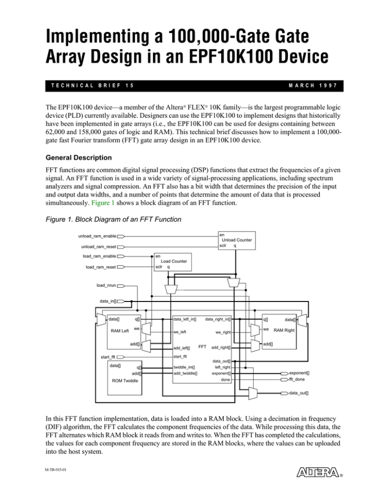
simultaneously. Figure 1 shows a block diagram of an FFT function.
Figure 1. Block Diagram of an FFT Function
en
Unload Counter
sclr
q
unload_ram_enable
unload_ram_reset
load_ram_enable
en
Load Counter
sclr q
load_ram_reset
load_nrun
data_in[]
data[]
RAM Left
q[]
we
data_left_in[]
data_right_in[]
we_left
add[]
add_left[]
we_right
FFT
add_right[]
q[]
data[]
we
RAM Right
add[]
start_fft
start_fft
data_out[]
data[]
q[]
add[]
ROM Twiddle
twiddle_im[]
add_twiddle[]
left_right
exponent[]
done
exponent[]
fft_done
data_out[]
In this FFT function implementation, data is loaded into a RAM block. Using a decimation in frequency
(DIF) algorithm, the FFT calculates the component frequencies of the data. While processing this data, the
FFT alternates which RAM block it reads from and writes to. When the FFT has completed the calculations,
the values for each component frequency are stored in the RAM blocks, where the values can be uploaded
into the host system.
M-TB-015-01
®
ALTERA MEGAFUNCTION PARTNERS PROGRAM
Functional Description
An FFT design with 256 points and 16-bit input and output data widths can be implemented into a single
EPF10K100 device. The FFT operates at clock frequencies of up to 38 MHz, which is comparable to
dedicated-off-the-shelf FFT devices. The FFT design also has the following features:
■
■
■
■
■
■
■
Uses the FLEX 10K look-up table (LUT) architecture to efficiently compute data
Uses two 256 × 32 RAM blocks to store data during computation
Uses a 128 × 32 ROM to store twiddle data, which is used during the FFT computation
Heavily pipelined, using the registers included in the FLEX 10K Logic Elements (LEs)
Contains many multipliers that use the FLEX 10K carry chain
Incorporates functions from the library of parameterized modules (LPM), which contains the most
efficient implementations of common functions, such as adders
Created in the Altera Hardware Description Language (AHDL™) format
FLEX 10K vs. Gate Array FFT Design
Using MAX+PLUS® II, the FFT design was compiled using an EPF10K100 device as the target device. The
same FFT design was compiled using an LSI Logic LCA500K gate array library with industry-standard
EDA tools (Synopsys Design Compiler and LSI Logic Memory Compiler). Table 1 shows the FFT design
requirements for both the EPF10K100 device and LCA500K gate array. For the LSI Logic LCA500K gate
array, a total of 106,929 gates is required for FFT design implementation.
Table 1. FFT Design Requirements for the EPF10K100 Device & LCA500K Gate Array
Design Components
EPF10K100 Device
LCA500K Gate Array
Two 256 × 32 RAMs
12 Embedded Array Blocks (EABs)
57,936 Gates
Logic
3,458 LEs
46,637 Gates
128 × 32 ROM
2,356 Gates
The EPF10K100 EABs implement memory functions more efficiently than the LCA500K gate array. To
implement memory for the FFT design, the EPF10K100 uses only 12 EABs, while the LCA500K uses over
60,000 gates for both RAM and ROM. Additionally, the EPF10K100 can efficiently implement registerintensive or highly pipelined designs, because each EPF10K100 LE contains a register. In contrast, the
LCA500K registers are assembled using NAND gates.
The documents listed below provide more detailed information. Part numbers are in parentheses.
■
■
fft Fast Fourier Transform Data Sheet (A-DS-FFT-01)
SB 12: Fast Fourier Transform MegaCore™ Function (A-SB-012-01)
You can request these documents from:
■
■
■
Altera Literature Services at (888) 3-ALTERA
Altera Express fax services at (800) 5-ALTERA
World-wide web at http://www.altera.com
Copyright 1997 Altera Corporation. Altera, AHDL, MegaCore, MAX, MAX+PLUS, MAX+PLUS II, FLEX, FLEX 10K, and EPF10K100 are
trademarks and/or service marks of Altera Corporation in the United States and/or other countries. Other brands or products are trademarks
of their respective holders. All rights reserved.
®
