Implementing
Dual-Port RAM
®
in FLEX 10K Devices
February 1996, ver. 1
Introduction
Application Note 65
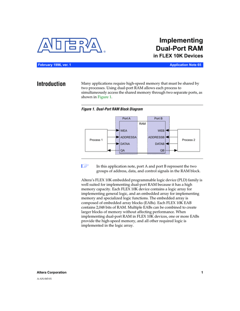
Many applications require high-speed memory that must be shared by
two processes. Using dual-port RAM allows each process to
simultaneously access the shared memory through two separate ports, as
shown in Figure 1.
Figure 1. Dual-Port RAM Block Diagram
Port A
Port B
RAM
WEA
Process 1
ADDRESSA
DATAA
QA
1
WEB
ADDRESSB
Process 2
DATAB
QB
In this application note, port A and port B represent the two
groups of address, data, and control signals in the RAM block.
Altera’s FLEX 10K embedded programmable logic device (PLD) family is
well suited for implementing dual-port RAM because it has a high
memory capacity. Each FLEX 10K device contains a logic array for
implementing general logic, and an embedded array for implementing
memory and specialized logic functions. The embedded array is
composed of embedded array blocks (EABs). Each FLEX 10K EAB
contains 2,048 bits of RAM. Multiple EABs can be combined to create
larger blocks of memory without affecting performance. When
implementing dual-port RAM in FLEX 10K devices, one or more EABs
provide the high-speed memory, and all other required logic is
implemented in the logic array.
Altera Corporation
A-AN-065-01
1
AN 65: Implementing Dual-Port RAM in FLEX 10K Devices
Two types of dual-port RAM can be implemented in FLEX 10K devices:
arbitrated and cycle-shared. Arbitrated dual-port RAM is useful for
designs that do not require both ports to frequently access the shared
memory at the same time. Arbitrated dual-port RAM requires complex
arbitration circuitry, but uses only one Clock. In contrast, cycle-shared
dual-port RAM allows two processes to simultaneously access the shared
memory through two separate ports. Cycle-shared dual-port RAM
requires two Clocks, and conserves device resources because it does not
require complex arbitration circuitry.
This application note describes how to implement cycle-shared dual-port
RAM in FLEX 10K devices.
f
Cycle-Shared
Dual-Port RAM
For more information about the FLEX 10K architecture, go to the
FLEX 10K Embedded Programmable Logic Family Data Sheet.
FLEX 10K devices use cycle-sharing to offer true dual-port RAM. To
implement cycle-sharing, the EAB must be clocked at twice the frequency
of the rest of the system, which allows both processes to access the dualport RAM within one system Clock cycle.
Figure 2 shows how cycle-shared dual-port RAM is implemented in
FLEX 10K devices.
2
Altera Corporation
AN 65: Implementing Dual-Port RAM in FLEX 10K Devices
Figure 2. FLEX 10K Cycle-Shared Dual-Port RAM Block Diagram
You can use the parameterized csdpram megafunction in MAX+PLUS II to set the address, data, and output ports to
variable widths. See “Software Support” on page 5 for more information.
EAB Note (1)
ADDRESSA
0
ADDRESSB
1
D
ADDRESS
Q
D
QA
ENA
DATAA
QB
0
DATAB
1
D
DATA
WEA
0
WEB
1
D
WE
VCC
CLOCK
D
D
CLOCKx2
Note:
(1)
Multiple EABs can be combined to create larger RAM.
Before the rising edge of the first clockx2 cycle, the address, data, and
Write Enable (we) inputs of port A are multiplexed onto the
corresponding inputs of the EAB. If the we signal is asserted, the rising
edge of clockx2 triggers the write pulse circuit within the EAB. Then, the
value of the dataa input is written to the EAB at the address specified by
the addressa input. If the we signal is not asserted, the EAB drives out the
data stored at the address specified by addressa. The data for port A is
latched at the EAB output by a register on the second rising edge of
clockx2.
On the rising edge of the first clockx2 cycle, the data, address, and we
inputs of port B are latched into registers, and are available on the rising
edge of the second clockx2 cycle.
Altera Corporation
3
AN 65: Implementing Dual-Port RAM in FLEX 10K Devices
Before the rising edge of the second clockx2 cycle, the address, data, and
we inputs of port B are multiplexed onto the corresponding inputs of the
EAB. If we is asserted, the rising edge of clockx2 triggers the write pulse
circuit within the EAB. The value of the datab inputs is written to the EAB
at the address specified by the addressb input. If we is not asserted, the
EAB drives out the data stored at that address. Because it is not latched,
the data from port B is always available to the system before the next
rising edge of the system Clock signal.
Clock skew between the two user-supplied Clocks lowers the maximum
operating frequency of the dual-port RAM. For example, a Clock skew of
2 ns adds 2 ns to the minimum Clock period. To accurately simulate this
behavior, Clock skew must be included in the simulation vectors by
introducing the two Clock sources as signals with a 2-ns delay; this Clock
skew can be introduced in MAX+PLUS II. MAX+PLUS II simulation does
not automatically show this reduction in performance because the Clock
skew is generated external to the device. Figure 3 shows the functional
waveform diagram for cycle-shared dual-port RAM in FLEX 10K devices.
Figure 3. FLEX 10K Cycle-Shared Dual-Port RAM Functional Waveforms
CLOCK
CLOCKx2
EAB WE
WEA (1)
EAB
ADDRESSA
ADDRESS
EAB DATA
QA
QB
WEB (2)
WEA (3)
ADDRESSB
ADDRESSA
ADDRESSB
ADDRESSA
DATAB
DATAA
DATAB
DATAA
QA1
QB (5)
DATAA
QA0
WEB (4)
QA1
QA1
QB (5)
Notes:
(1)
(2)
(3)
(4)
(5)
4
When port A is requesting a read, wea = 0.
When port B is requesting a write, web = 1.
When port A is requesting a write, wea = 1.
When port B is requesting a read, web = 0.
qb is valid only at the end of cycle. The EAB output is not re-registered when it
drives qb.
Altera Corporation
AN 65: Implementing Dual-Port RAM in FLEX 10K Devices
Collision
Collision occurs when both processes attempt to access the shared
memory location at the same time. When port A and port B attempt to
write data to the same memory address simultaneously, non-cycle-shared
dual-port RAM requires complex arbitration circuitry to identify which
process accesses the memory.
With cycle-shared dual-port RAM, if port A and port B write to the same
address simultaneously, the data from port B is stored. If port A writes to
the memory address that port B is reading, a busy signal informs the
system that the data at that particular address has changed since the last
Clock cycle. Figure 4 shows how the busy signal is generated.
Figure 4. Generation of Busy Signal
ADDRESSA
ADDRESSB
BUSY
WEA
Software
Support
You can implement cycle-shared dual-port RAM in FLEX 10K devices
with a megafunction provided with Altera’s MAX+PLUS II development
system. The megafunction, csdpram, incorporates parameterized
functions from the library of parameterized modules (LPM). The LPM is
an architecture-independent library of logic functions that completely
describes the logic operation of digital circuits. Because all LPM functions
have configurable parameters, you can control the size of csdpram to meet
your design requirements. Figure 5 shows the symbol for the csdpram
megafunction.
The csdpram megafunction has the following parameters:
■
■
■
Altera Corporation
LPM_WIDTH is the word size of the dual-port RAM.
LPM_WIDTHAD is the number of address lines in the dual-port RAM.
LPM_NUMWORDS is the depth of the dual-port RAM. If LPM_NUMWORDS
is not specified, the csdpram depth defaults to 2^LPM_WIDTHAD.
5
AN 65: Implementing Dual-Port RAM in FLEX 10K Devices
Figure 5. csdpram Megafunction Symbol
LPM_NUMWORDS =
LPM_WIDTH =
LPM_WIDTHAD =
CSDPRAM
DATAA[]
DATAB[]
ADDRESSA[]
ADDRESSB[]
QA[]
WEA
QB[]
WEB
BUSY
CLOCK
CLOCKx2
Table 1 lists the input and output ports of csdpram.
Table 1. csdpram Ports
Pin Type
6
Ports
Description
Input
dataa
Data to be written to port A.
Input
datab
Data to be written to port B.
Input
wea
Write enable input to port A.
Input
web
Write enable input to port B.
Input
addressa
Memory address accessed by port A.
Input
addressb
Memory address accessed by port B.
Input
clock
System Clock.
Input
clockx2
Internal Clock of the dual-port RAM (must operate at
twice the frequency of the system Clock).
Output
qa
Data output from port A.
Output
qb
Data output from port B. qb is valid only at the end of
cycle.
Output
busy
Indicates addressa = addressb and wea is
asserted.
Altera Corporation
AN 65: Implementing Dual-Port RAM in FLEX 10K Devices
Conclusion
Altera Corporation
You can use the FLEX 10K EAB to quickly and efficiently implement dualport RAM and other memory functions. Altera’s MAX+PLUS II
development system provides the csdpram megafunction, which allows
you to implement cycle-shared dual-port RAM and create flexible designs
for a variety of applications.
7
AN 65: Implementing Dual-Port RAM in FLEX 10K Devices
®
2610 Orchard Parkway
San Jose, CA 95134-2020
(408) 894-7000
Applications Hotline:
(800) 800-EPLD
Customer Marketing:
(408) 894-7104
Literature Services:
(408) 894-7144
8
Altera, MAX, MAX+PLUS, and FLEX are registered trademarks of Altera Corporation. The following are
trademarks of Altera Corporation: MAX+PLUS II and FLEX 10K. Altera acknowledges the trademarks of
other organizations for their respective products or services mentioned in this document. Altera products are
protected under numerous U.S. and foreign patents and pending applications, maskwork rights, and
copyrights. Altera warrants performance of its semiconductor products to current specifications in accordance
with Altera’s standard warranty, but reserves the right to make changes to any products
and services at any time without notice. Altera assumes no responsibility or liability
arising out of the application or use of any information, product, or service described
herein except as expressly agreed to in writing by Altera Corporation. Altera customers
are advised to obtain the latest version of device specifications before relying on any
published information and before placing orders for products or services.
Copyright 1996 Altera Corporation. All rights reserved.
Altera Corporation
Printed on Recycled Paper.


