news & views
GRAPHENE
Show of adhesive strength
The adhesion energies for atomically thin graphene membranes on silicon dioxide substrates have now been measured.
Rui Huang
© VICTOR AND REX TZEN
G
raphite is composed of layers of
carbon atoms that are held together
by strong covalent bonds within
each graphene layer and relatively weak
van der Waals forces between the layers.
The mechanical properties of graphite —
it is anisotropic and prone to interlayer
cleavage — are closely related to the
characteristics of these forces. Furthermore,
according to recent work at the University of
Colorado in Boulder, van der Waals forces
could also be responsible for the ultrastrong
adhesion between atomically thin graphene
membranes and a silicon oxide substrate1.
Writing in Nature Nanotechnology,
Scott Bunch and co-workers report that the
adhesion energy for monolayer graphene
on silicon oxide is higher than that for
membranes containing between two and
five layers of graphene. Although the
physical origin for this difference is not
fully understood, the team suggests that
the extreme flexibility of the monolayer
graphene may be responsible.
Measurement of the interfacial adhesion
energy is essential for practical applications
of graphene in integrated electronic and
mechanical devices. Previously, researchers
at the University of Maryland estimated
the graphene–SiO2 adhesion energy to be
0.096 J m–2, based on the interlayer van der
Waals interaction in graphite2, and a team at
Northeastern University reported an average
value of 0.151 J m–2 for multilayer graphene
sheets (roughly five layers) on a silicon wafer,
which was obtained with a nanoparticle
intercalation method3. The values reported by
Bunch and colleagues are higher — 0.31 J m–2
for membranes containing two to five layers
of graphene — because they are based on
independent measurements of the Young’s
modulus of the membranes4, whereas the
measurements at Northeastern University
used smaller values for Young’s modulus. This
ability to independently measure both the
Young’s modulus and the adhesion energy
is an important advantage of the method
developed by Bunch and co-workers, which
is based on the pressurized blister test (also
known as the bulge test).
Pressurized blister tests are routinely used
to measure the mechanical properties of
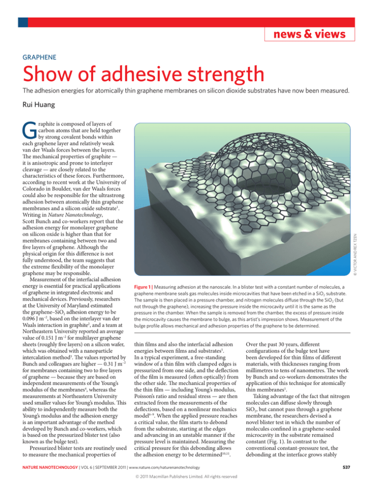
Figure 1 | Measuring adhesion at the nanoscale. In a blister test with a constant number of molecules, a
graphene membrane seals gas molecules inside microcavities that have been etched in a SiO2 substrate.
The sample is then placed in a pressure chamber, and nitrogen molecules diffuse through the SiO2 (but
not through the graphene), increasing the pressure inside the microcavity until it is the same as the
pressure in the chamber. When the sample is removed from the chamber, the excess of pressure inside
the microcavity causes the membrane to bulge, as this artist’s impression shows. Measurement of the
bulge profile allows mechanical and adhesion properties of the graphene to be determined.
thin films and also the interfacial adhesion
energies between films and substrates5.
In a typical experiment, a free-standing
window of a thin film with clamped edges is
pressurized from one side, and the deflection
of the film is measured (often optically) from
the other side. The mechanical properties of
the thin film — including Young’s modulus,
Poisson’s ratio and residual stress — are then
extracted from the measurements of the
deflections, based on a nonlinear mechanics
model6–9. When the applied pressure reaches
a critical value, the film starts to debond
from the substrate, starting at the edges
and advancing in an unstable manner if the
pressure level is maintained. Measuring the
critical pressure for this debonding allows
the adhesion energy to be determined10,11.
NATURE NANOTECHNOLOGY | VOL 6 | SEPTEMBER 2011 | www.nature.com/naturenanotechnology
© 2011 Macmillan Publishers Limited. All rights reserved
Over the past 30 years, different
configurations of the bulge test have
been developed for thin films of different
materials, with thicknesses ranging from
millimetres to tens of nanometres. The work
by Bunch and co-workers demonstrates the
application of this technique for atomically
thin membranes1.
Taking advantage of the fact that nitrogen
molecules can diffuse slowly through
SiO2, but cannot pass through a graphene
membrane, the researchers devised a
novel blister test in which the number of
molecules confined in a graphene-sealed
microcavity in the substrate remained
constant (Fig. 1). In contrast to the
conventional constant-pressure test, the
debonding at the interface grows stably
537
news & views
in the blister test with a constant number
of molecules, which allows the radius of
the blister (which is increasing) and the
internal pressure (which is decreasing) to be
measured continuously.
As such, these measurements provide a
comprehensive data set for the mechanical
and adhesion properties of graphene
membranes. In particular, the adhesion
energy can be determined directly from
the measurable quantities, without any
need to assume the value of Young’s
modulus (although it is necessary to
assume a Poisson’s ratio). Moreover,
the Young’s modulus of the membrane
can be determined separately using the
measured deflection. Furthermore, by
using a different geometry for the cavity,
it should also be possible to determine
Poisson’s ratio for the graphene membrane9.
The robustness of this technique opens
up ample opportunities for fundamental
studies on the nanomechanics of graphene
interacting with other materials.
The measured adhesion energy for
monolayer graphene is surprisingly high
(~0.45 J m–2). As pointed out by Bunch and
co-workers, this may be attributed to the
flexibility of monolayer graphene. It has
been predicted that the bending modulus
of monolayer graphene is two orders
of magnitude lower than that of bilayer
graphene12, which could lead to monolayer
and multilayer graphene membranes having
different morphologies on the SiO2 substrate
and, hence, different adhesion energies.
Theoretical models have predicted
that graphene membranes supported
on a surface can undergo a transition
between a highly conformal morphology
and a non-conformal morphology,
depending on the surface roughness
and the bending modulus of the
membrane13,14. The adhesion energy, as
measured by the blister test, tells us about
the microscopic interactions between
graphene and the substrate. As monolayer
graphene conforms much more closely
to the substrate surface than membranes
containing two to five layers, the measured
adhesion energy is expected to be higher. A
more quantitative analysis may be required
to confirm this explanation, and to provide
a better understanding of the effects of
surface forces, roughness and the intrinsic
mechanical properties of graphene on
interfacial adhesion.
Ultimately, for graphene to be integrated
into devices, its adhesive interactions
with other materials (such as metals
and polymers) will have to be studied in
detail. Both experimental techniques and
theoretical models are needed to uncover
the physical mechanisms that may result in
different levels of adhesive interactions15.
The impacts of the adhesive interactions on
the fabrication, performance and reliability
of graphene devices will also have to be
examined, as has happened with thinfilm devices.
❐
Rui Huang is in the Department of Aerospace
Engineering and Engineering Mechanics, University
of Texas at Austin, Austin, Texas 78712, USA.
e-mail: ruihuang@mail.utexas.edu
References
Koenig, S. P. et al. Nature Nanotech. 6, 543–546 (2011).
Ishigami, M. et al. Nano Lett. 7, 1643–1648 (2007).
Zong, Z. et al. J. Appl. Phys. 107, 026104 (2010).
Lee, C. et al. Science 321, 385–388 (2008).
Freund, L. B. & Suresh, S. Thin Film Materials (Cambridge Univ.
Press, 2003).
6. Vlassak, J. J. & Nix, W. D. J. Mater. Res. 7, 3243–3249 (1992).
7. Williams, J. G. Int. J. Fracture 87, 265–288 (1997).
8. Wan, K. T. et al. Thin Solid Films 425, 150–162 (2003).
9. Xu, D. & Liechti, K. M. Exp. Mech. 50, 217–225 (2010).
10.Gent, A. N. & Lewandowski, L. H. J. Appl. Polymer Sci.
33, 1567–1577 (1987).
11.Allen, M. G. & Senturia, S. D. J. Adhesion 25, 303–315 (1988).
12.Koskinen, P. & Kit, O. O. Phys. Rev. B 82, 235420 (2010).
13.Li, T. & Zhang, Z. J. Phys. D 43, 075303 (2010).
14.Aitken, Z. H. & Huang, R. J. Appl. Phys. 107, 123531 (2010).
15.Sabio, J. et al. Phys. Rev. B 77, 195409 (2008).
1.
2.
3.
4.
5.
BIOMATERIALS
A natural source of nanowires
Fibrous proteins from bacteria can be used to make biofilms with electrical conductivities that are comparable to
those measured in conducting polymers.
Fang Qian and Yat Li
T
he discovery of conducting
polymers1 in the mid-1970s led to the
development of a variety of organic
electronic and optoelectronic devices,
including light-emitting diodes, transistors
and solar cells. If we consider conducting
polymers to be ‘synthetic organic metals’, we
can ask if the discovery of ‘natural organic
metals’ could have similar consequences.
Biological proteins are obvious candidates
for ‘natural organic metals’. If we could
understand long-range charge transport
in these materials, then we might be able
to introduce metal or semiconducting
biomaterials2 to electronic devices and open
up new opportunities in bioelectronics,
bioenergy and medical applications.
Pilin nanofilaments (pili) — also
known as microbial nanowires — are a
class of fibrous proteins found in sediment
538
bacteria, and researchers have been
investigating charge transport in these
quasi-one-dimensional biomaterials for a
number of years. The first step was taken
by Derek Lovely, Mark Tuominen and coworkers at the University of Massachusetts
in 2005, when they used an atomic force
microscope with a conducting probe to
measure the conductance maps of pilin
nanofilaments taken from Geobacter
sulfurreducens on a graphite electrode3.
The researchers found that the pili were
conducting in the radial direction, which
indicated that they might be involved in
extracellular electron transfer.
A year later, Yuri Gorby, of the
Pacific Northwest National Laboratory,
and co‑workers examined the pilin
nanofilaments produced by the MR-1
strain of Shewanella oneidensis with a
combination of scanning tunnelling
microscopy and spectroscopy 4. The
scanning tunnelling microscopy images
(based on tunnelling current) showed that
these pili were also highly conducting in
the radial direction, which suggested that
radial conductivity might be a generic
feature of the pili from certain types of
bacteria. However, the measurement
techniques available at the time were
not able to quantitatively investigate the
conductivity of pili along their length.
Now, writing in Nature Nanotechnology,
Tuominen, Lovely and co-workers
report that films made of pili taken from
G. sulfurreducens exhibit metallic-like
conductivities and are able to conduct an
electric current over centimetre distances5.
The UMass team designed a unique
microbial fuel-cell reactor with a split
NATURE NANOTECHNOLOGY | VOL 6 | SEPTEMBER 2011 | www.nature.com/naturenanotechnology
© 2011 Macmillan Publishers Limited. All rights reserved
