MODELING, DESIGN AND FABRICATION OF A NOVEL ELECTROWETTING BASED IMPINGEMENT COOLER
advertisement
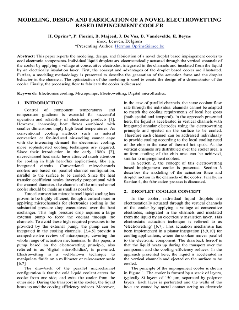
MODELING, DESIGN AND FABRICATION OF A NOVEL ELECTROWETTING BASED IMPINGEMENT COOLER H. Oprins*, P. Fiorini, B. Majeed, J. De Vos, B. Vandevelde, E. Beyne imec, Leuven, Belgium *Presenting Author: Herman.Oprins@imec.be Abstract: This paper reports the modeling, design, and fabrication of a novel droplet based impingement cooler to cool electronic components. Individual liquid droplets are electrostatically actuated through the vertical channels of the cooler by applying a voltage at consecutive electrodes, integrated in the channels and insulated from the liquid by an electrically insulation layer. First, the concept and advantages of the droplet based cooler are illustrated. Further, a modeling methodology is presented to describe the generation of the actuation force and the droplet behavior in the channels. The optimization of the modeling is used to create the design of a demonstrator of the cooler. Finally, the processing flow to fabricate the cooler is discussed. Keywords: Electronics cooling, Micropumps, Electrowetting, Digital microfluidics. 1. INTRODUCTION Control of component temperatures and temperature gradients is essential for successful operation and reliability of electronics products [1]. However, increasing heat fluxes combined with smaller dimensions imply high local temperatures. As conventional cooling methods such as natural convection or fan-induced air-cooling cannot cope with the increasing demand for electronics cooling, more sophisticated cooling techniques are required. Since their introduction in the early 1980s [2], microchannel heat sinks have attracted much attention for cooling in high heat-flux applications, like e.g. integrated circuits. Conventional microchannels coolers are based on parallel channel configuration, parallel to the surface to be cooled. Since the heat transfer coefficient scales inversely proportional with the channel diameter, the channels of the microchannel cooler should be made as small as possible. Forced convection microchannel liquid cooling has proven to be highly efficient, though a critical issue in applying microchannels for electronics cooling is the substantial pressure drop encountered over the heat exchanger. This high pressure drop requires a large external pump to force the coolant through the channels. To avoid these high required pressures to be provided by the external pump, the pump can be integrated in the cooling channels. [3,4,5] provide a comprehensive review of micropumps, covering the whole range of actuation mechanisms. In this paper, a pump based on the electrowetting principle, also referred to as ‘digital microfluidics’, is presented. Electrowetting is a well-known technique to manipulate fluids on a millimeter or micrometer scale [6,7]. The drawback of the parallel microchannel configuration is that the cold liquid coolant enters the cooler from one side, and exits the cooler from the other side. During the transport in the cooler, the liquid heats up and the cooling efficiency reduces. Moreover, in the case of parallel channels, the same coolant flow rate through the individual channels cannot be adapted to match the cooling requirements of local hot spots (both spatial and temporal). In the approach presented here, the liquid is accelerated in vertical channels with integrated annular electrodes using the electrowetting principle and ejected on the surface to be cooled. Therefore each channel can be addressed individually to provide cooling according to the local cooling need of the chip in the case of thermal hot spots. As the vertical channels are distributed over the cooler area, a uniform cooling of the chip area can be achieved, similar to impingement coolers. In Section 2, the concept of this electrowetting based impingement cooler is presented. Section 3 describes the modeling of the actuation force and droplet motion in the channels of the cooler. Finally, in Section 4, the fabrication process is discussed. 2. DROPLET COOLER CONCEPT In the cooler, individual liquid droplets are electrostatically actuated through the vertical channels of the cooler by applying a voltage at consecutive electrodes, integrated in the channels and insulated from the liquid by an electrically insulation layer. This electrostatic actuation technique is referred to as ‘electrowetting’ [6,7]. This actuation mechanism has been implemented in a planar integration [8,9,10] for cooling applications, where the coolant moves parallel to the electronic component. The drawback hereof is that the liquid heats up during the transport over the component and the cooling efficiency reduces. In the approach presented here, the liquid is accelerated in the vertical channels and ejected on the surface to be cooled. The principle of the impingement cooler is shown in Figure 1. The cooler is formed by a stack of layers, typically Si layers of 150 µm, separated by polymer layers. Each layer is perforated and the walls of the hole are coated by metal contact acting as electrode and by an insulating layer. The metal layers are routed to the periphery of the chip in such a way that a voltage can be easily applied to the electrodes. Layers are stacked on top of each other by using a polymer adhesive, in such a way that the holes form a plurality of vertical microchannels. Each vertical microchannel has now a series of electrodes which can be used to transport droplets by electrostatic actuation along the channel itself. The layer stack is glued to the chip to be cooled. In this way the same device combines the fluidic microchannels and the pump. Fig. 1: Schematic representation of the electrowetting based impingement cooler. 3D droplet cooler Chip Heat Exchanger simulations as a function of the system parameters including actuation voltage, insulator properties (thickness, permittivity), droplet volume, channel diameter and electrode pitch, spacing and geometry. A general formulation for the electrostatic force has been derived and implemented in the modeling flow. The total electrostatic energy U el in the system, with a volume Vol, is given by = U el 1 ∫ E ⋅ DdVol 2 Vol (1) where E is the electric field and D is the electric displacement. The electrostatic actuation force acting on the droplet can be calculated as the negative gradient of the energy variation. The system tends to move towards a situation of minimal energy. In the case where only the contribution of the electric energy to the total energy is considered, the change in total energy can be written as follows: (2) dW = −dU el Because only the horizontal component of the electrostatic force contributes to the moving of the droplet, the net actuation force is given by F= dU el . dx (3) Fig. 3 shows the effect of the channel diameter and droplet volume on the net actuation force acting on a droplet in the vertical channel. A similar analysis is performed for the other system parameters, to allow an optimization in order to achieve a maximal actuation force. Secondary Coolant Fig. 2: Schematic representation of the closed loop cooling system. The presented cooler is part of a closed loop cooling system. This system is represented schematically in figure 2. The cold liquid (‘coolant’) enters the primary cooler, e.g. through a manifold described later. Next, the liquid is actuated as droplets through the vertical cylindrical channels and sprayed onto the surface of the chip. At the outlet of the cooler, the heated droplets are collected and removed from the primary cooler. Subsequently, the liquid is cooled by a secondary cooler (heat exchanger). This heat exchanger can be at another location in the system, where more heat transfer area can be foreseen. Afterwards, the cooled liquid is fed back to the cooler where new droplets are dispensed and sprayed onto the chip. 3. THEORY 3.1. Actuation force calculation The actuation force, acting on the droplet during transition through the vertical channel in the cooler, is modeled using quasi-static electrostatic finite element Fig. 3: Simulation results for the actuation force on a droplet in cylindrical channel: effect of the channel diameter (top) and droplet length (bottom). model, a robust switching scheme can be found for the voltage values and frequency to guarantee a continuous droplet movement to the channel of the cooler. This dynamic model and the electrostatic modeling are then used to optimize the system parameters to achieve a maximal droplet flow rate. The modeling results are used to design a demonstrator for the droplet flow in the vertical channels. In that design, various channel diameters (100 μm to 500 μm) are foreseen to validate the modeling results. 4. FABRICATION Fig. 4: Simulation result for the droplet position in the vertical channel for a switching frequency of 50 Hz. 3.2. Dynamic droplet motion modeling Further, an analytic dynamic model, based on the simulations results of the electrostatic force and on empirical models for the static and dynamic contact line friction force, is presented. The dynamic model predicts the transient droplet response the droplet velocity and achievable flow rates for a voltage application, and allows optimization of the switching voltage from one electrode to the next. In the analytical model, the droplet is considered as a single discrete mass moving through the channel. The onedimensional force balance can be written as follows: M with: dU av = Fel − FW − FCL − FD dt In this section we present a simplified version of the device described in section 2. The device cross sections are shown in Fig. 5. The 3D schematics, together with a photograph of the fabricated dies are shown in Fig. 6. The four stacked layers are made of low resistivity Si (5 mΩ/cm), and their sides are increasing from top to bottom. The large Si conductivity allows controlling the potential around each section of the channel without implementing a complex metal routing; the variable side allows contacting each layer without the use of through silicon via. The simplified version can be easily fabricated and allows studying the behavior of the droplets in the channel, but control of individual channels cannot be achieved. (4) M: Uav : Fel : Fw : mass of the droplet; average velocity of the droplet; electrostatic driving force; shear force between the droplet and the channel; FCL : contact-line friction force; FD : drag force on filler liquid; D: the channel diameter; L: the droplet length; µ: the viscosity of the coolant; µfiller: the viscosity of the host medium; z contact line friction coefficient The forces acting on the droplet can be written as a function of the droplet location and/or velocity. The electrostatic force is known from the simulations as a function of the droplet location. The other forces can be written as follows [11]: U av π DL D = FCL , static min Fel , γ (5) FW = 4 µ ( LV [ cos (θ ) − cos (θ )] R A max, static πD ) (6) FCL , dynamic = ζ U av 2π D (7) a F= µ filler ⋅ ⋅ H ⋅ U D 2 (8) As a result, the differential equation (4), that describes the droplet behavior, and can be solved for the droplet position. Fig. 3 shows the result for voltage application over three consecutive electrodes. With this dynamic Silicon Oxide Adhesive Fig. 5: Cross section of the fabricated device. Fig. 6: 3D schematics (left) and photograph (right) of the fabricated device. The fabrication process flow is shown in Fig. 7. First circular channels about 300 um deep are excavated in Si by means of DRIE (Fig. 7a). Channel diameter varies from 100 to 300 um. Spacing is fixed to 100um. Then an insulating layer (TEOS) is deposited in order to coat the channels (Fig. 7b). Deposition conditions are tuned in order to minimize oxide thickness variation in the vertical direction inside the channels. The oxide layer is opened in order to access the Si layers. Metal contacts are deposited and patterned (see Fig. 7c). The processed wafer is bonded to a carrier wafer by using an adhesive (HT1010......), which can be removed later in a solvent (see Fig. 7c). The wafer is then grinded to the required thickness, 150 um (see Fig. 7e) and an oxide layer is deposited at a very low temperature (450 K), to avoid de-bonding of the device wafer from the carrier wafer (see Fig. 7f). Finally an adhesive layer (RoHS) is spun and patterned as shown in Fig. 7g. The device and the carrier wafers are then diced together and separated by soaking them in the glue solvent for a few hours. Dies have typical dimensions of about 4mm x 5mm. The largest die is bonded to a special support (a cavity excavated in a Si Wafer) as shown in Fig. 6. The second, third and fourth die are then subsequently bonded, as shown for die #2 in Fig. 6. A photograph of the fabricated device is shown Fig. 6. a) Deep reactive ion etch of holes b) c) TEOS deposition TEOS opening, Al deposition and patterning i)Die #2 bonded to die #1 Fig. 7: Process flow. See text for description. 5. CONCLUSIONS This paper reports the modeling, design, and fabrication of a novel droplet based impingement cooler to cool electronic components. Individual liquid droplets are electrostatically actuated through the vertical channels of the cooler by applying a voltage at consecutive electrodes, integrated in the channels and insulated from the liquid by an electrically insulation layer. In this paper, the concept of the cooler is first discussed. Further, a modeling methodology is presented. This mythology allows optimization of the system parameters to achieve a maximum actuation force and a maximum droplet flow rate. Based on the results of the modeling optimization study, a design for a demonstrator of the droplet cooler has been made. Finally, the processing flow to fabricate this demonstrator has been described. The demonstrator will be used to validate the modeling results. ACKNOWLEDGEMENTS This work was supported by the SBO project 060830 HyperCool-IT funded by IWT-Vlaanderen. REFERENCES d) Adhesive bonding to a carrier wafer e) f) Wafer grinding Protection oxide deposited at low temperature g) Adhesive layer deposition and patterning h) Die #1 bonded to the Silicon support [1] Lasance C 2003 Thermally driven reliability issues in microelectronic systems: status-quo and challenges Microelectronics Rel. 43 1969-1975 [2] Tuckerman DB, Pease RFW 1981 High-Performance Heat Sinking for VLSI IEEE EDL 2 126 [3] Nguyen NT et al. 2002 MEMS-micropumps: a review. J. Fluids Eng 124(2):384-392 [4] Laser DJ, Santiago JG 2004 A review of micro-pumps J. Micromech. Microeng 14(6):35-64 [5] Iverson BD, Garimella SV 2008 Recent advances in microscale pumping technologies J. Microfluid. Nanofluid 5:45-174 [6] Mugele F, Baret JC 2005 J. Phys.: Condens. Matter 17 R705-R774 [7] Pollack MG, Fair RB, Shenderov AD 2000 Appl. Phys. Lett. 77 1725-1726 [8] Pamula VK Chakrabarty K 2003 Proc. ACM Great Lakes Symposium on VLSI 84-87. [9] Oprins H et al. 2004 THERMINIC 207-212 [10] Mohseni K 2005 SEMITHERM 21 20-25 [11] Oprins H 2010 Selective cooling of electronics using electrostatically actuated liquid droplets, PhD dissertation, K.U.Leuven
