PN-GENERATORS EMBEDDED IN HIGH PERFORMANCE SIGNAL PROCESSORS Dresden University of Technology
advertisement
PN-GENERATORS EMBEDDED IN HIGH PERFORMANCE SIGNAL PROCESSORS
Ulrich Walther and Gerhard P. Fettweis
Dresden University of Technology
Mannesmann Mobilfunk Chair for Mobile Communications Systems
Mommsenstr. 13, D-01062 Dresden, Germany
ABSTRACT
Wireless systems based on CDMA such as proposed in the 3GPP
standard utilize pseudo random number sequences for generation
of the spreading codes. These sequences are usually created by the
use of finite field arithmetic. A pure software implementation onto
a digital signal processor (DSP) is very inefficient and would result
in unreasonable high computational load. In this paper a hardwarebased scheme is proposed which allows for an efficient implementation on a high performance DSP as well as into an ASIC. With
the configurable approach a binary PN-sequence with an arbitrary
primitive polynomial can be generated. The unit was specially designed for and embedded into a domain specific processor, which
supports W-CDMA and alike baseband processing.
1. INTRODUCTION
The wireless communication standard 3GPP represents a Wideband CDMA system. At the transmitter the original data is spread
by means of a special sequence, the spreading code. The spreading
operation increases the signal bandwidth and enables user and cell
separation.
At the receiver side the sampled data is fed into a RAKE receiver to cope with multi-path propagation channels. The RAKE
embodies a set of “fingers” each of them performing a de-spread
operation: the incoming data will be multiplied by the conjugate
code sequence. The fingers need to correlate the data and the code
with different input delays according to the channel impulse response. This can be achieved by buffering the input data and
feeding the fingers appropriately. However, a large buffer memory might result which is rather unfavorable for a DSP-solution.
Another approach eliminates the need for this by starting the code
sequences for each finger with a different delay, i.e. the code phase
for each finger differs.
A software solution in a standard processor would increase the
algorithms complexity by about 100% raising the computational
requirements to an infeasible measure. Therefore, we are looking
for a hardware-based code generation which free the processor for
further computations. However, since this hardware is required for
the spreading operation only the extensions should add as little to
the core size as possible.
In this paper we present an architecture with a minimum additional hardware area which is independent from the generating
polynomial over GF(2m ), m ≤ 32. Simple control matched to
the instruction set of the processor is accomplished by memory
This work was supported by Deutsche Forschungsgemeinschaft contract SFB 358-A6
mapped configuration registers accessible via standard move instructions.
Section 2 explains the generation of PN-sequences and introduces a mathematical formulation in order to derive different
forms of such sequence generators and modifications thereof. The
implementation and embedding of the proposed circuit in a DSPdata-path is outlined in Section 3. Finally some results and a comparison of different realizations will be given.
2. PN-SEQUENCE GENERATION
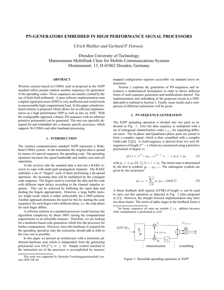
The 3GPP spreading operation is divided into two parts as indicated in Fig. 1. First the data sequence is multiplied with a
set of orthogonal channelization codes cch,i for separating different users. The In-phase and Quadrature-phase parts are joined to
form a complex signal, which is then scrambled with a complex
Gold-code [1][2]. A Gold-sequence is derived from two real Msequences of length 2m −1 which are constructed using a primitive
polynomial of degree m
p(x) = xm + pm−1 xm−1 + · · · + p1 x + p0
(1)
with p0 = 1, pi {0, 1}, 0 < i < m. The initial state is determined
by the first m symbols y0 . . . ym−1 . The subsequent symbols are
given by the recurrence1
X
m−1
yk+m =
pi yk+i (mod 2)
(2)
i=0
A linear feedback shift register (LFSR) of length m can be used
to carry out this operation as depicted in Fig. 2 (also proposed
in [1]). However, the straight forward implementation may have
two draw-backs: The series of adder stages in the feedback forms a
1 for binary sequences all sums are modulo 2, i.e. addition becomes
XOR, multiplication is performed as AND
Cscr,n
I
DP CHm
S
P
cch,SF,m
Q
∗j
channelization
scrambling
Figure 1: Downlink spreading operation in 3GPP
long critical path and, more serious, the initialization of the register
becomes difficult.
The initial state of the register is determined by two parameters: the code number and the delay/offset with respect to other
RAKE fingers. In 3GPP uplink mode the binary representation of
the code number directly determines the initial state and the offset
tells how many times the shift register need to be pulsed before the
first valid symbol is available at the output. In the downlink case
the sum of code number and offset defines how many times the
register need to be pulsed starting with the initial vector s(0) . For
large offsets or code numbers it would take a long time to “preset”
the generator. Alternatively one could use a look-up table where
the states of the register are stored for different offset values. Again
for large offsets this solution is not practicable since the memory
size becomes unreasonably large. A much smarter solution would
calculate the initial state within a few cycles - finite field arithmetic
need to be implemented.
One way to produce an offset in the sequence output is the use
of the LFSR with a mask that multiplies the contents of the memory elements with the masking coefficients and adding the results
up (see Fig. 3). This procedure is proposed in the standard [1] to
create a half-period phase shifted version of the original sequence
for the quadrature parts. However, in order to produce an arbitrary offset the masking value b needs to be re-calculated for each
initialization.
Mathematically the state of the LFSR at time k can be de(k) (k) (k)
(k)
scribed by the vector s(k) = [s0 s1 s2 . . . sm−1 ]T . After
one clock pulse the state changes into
s(k+1) = M s(k)
0
B
B
B
M=B
B
@
(3)
with the transition matrix
pm−1
1
0
..
.
0
pm−2
0
1
..
.
0
. . . p1
... 0
... 0
.
. . . ..
... 1
1
0
0
..
.
0
1
CC
CC
CA
(4)
Setting k = 0 in (5) and merging with (6) generates
b(q) = (MT )q b(0)
Hence a circuit for exponentiation of the matrix M is required [3].
A popular solution to that problem is the use of a Galois Field
(GF) multiplier. Consider the transposed form of the LFSR shown
in Fig. 4. That circuit is also known as modular feedback shift
register (MFSR) [4].
The state of the MFSR at time q should be defined with b(q) .
Than the subsequent state is given by
b(q+1) = MT b(q)
(q)
pm−2
pm−3
s0
s1
pm−2
s1
s2
(q)
mask
(6)
b0
s2
out
yk+m−1
sm−1
(q)
yk
(q)
b2
bm−1
Figure 3: Linear feedback shift register with mask
pm−1
=1
yk
(q)
b1
pm−3
yk+q
p0
sm−1
yk+m
pm−1
s0
where q is the offset between the sequences. The special case of
b(0) = [0 0 . . . 0 1]T produces zero offset. In order to determine
the mask b(q) we substitute the recursion (3) and the output yields
pm−1
(9)
In terms of Galois Field arithmetics each state of the MFSR represents an element of the field2 . Furthermore every field element
can be expressed as a power of a primitive element α, i.e. s̃(0) =
α0 , s̃(1) = α, . . . , s̃(i) = αi . Each clock cycle the register advances its state to the next higher power of the primitive element.
Therefore the MFSR is referred to as α-multiplier.
If the MFSR is extended according to Fig. 5, the circuit could
multiply arbitrary numbers of GF(2m ) in a serial manner, hence it
is known as GF-multiplier [5]. First the shift register is initialized
with the all-zero state. Each clock cycle the partial product vector
xi y is added to the actual state. The xi are the subsequent components of the x-operand starting with the most significant bit. After
m cycles the product is available.
(5)
(q)
(q)
b0 = sm−1 .
(k)
yq = sm−1 = [0 0 . . . 0 1] Mq s(0)
(8)
with M being the same matrix as for the LFSR. The recursion can
easily be transformed into expression (7). Thus the state of the
MFSR is identical to the mask value b if the initial state b0 holds
the above mentioned condition. Furthermore the outputs of the
MFSR and the LFSR are equivalent if s(0) = [1 0 . . . 0]T , hence
The output yk equals sm−1 . The shifted output caused by the mask
(q) (q)
(q)
b(q) = [b0 b1 . . . bm−1 ]T results in
yq+k = (b(q) )T s(k)
(7)
pm−2
p0
bm−1
yk
out
pm−3
b0
b1
b2
yk
s = [s0 s1 s2 . . . sm−1
]T
Figure 4: Modular feedback shift register
Figure 2: Linear feedback shift register
2 please
refer to [5][6][7] for a detailed description of GF(2m )
The multiplier circuit is used to create an element αn by forming it from previously calculated and stored values αni using the
relation
αn =
Y
L−1
αni
X
L−1
with n =
i=0
nk ,
(10)
(9) leads to the LFSR state
0
b
B
b
B
=B
B
@
s̃(q)
i=0
(q+m−1)
0
(q+m−2)
0
..
.
(q)
b0
P
i.e. the power is generated as a series of multiplications. Example:
i
Assume the binary representation of the number n = L−1
i=0 ni 2 ,
ni ∈ {0, 1}. Now the product calls always for values of the form
i
α2 . In this case L = m holds, which equals the total number
of α-powers to be stored. However, the number of multiplications
increases to m, hence the total number of cycles for the initialization becomes m2 . That value can be reduced at the cost of an
increased memory size if the number n is represented with a higher
order number system (e.g. octal, O = 8) and a group of bits defines the value of a digit ni (e.g. 3=ld(O)=ld(8)). The total storage
for an m-bit number becomes mem = dm/ld(O)e × O with O
being the order of the system. Now only m/ld(O) multiplications
are required. The tradeoff between memory size and intitialization
time should be considered in the final implementation.
Now the overall PN-generator becomes a combination of a
LFSR (Fig. 3) and a GF-multiplier according to Fig. 5 which generates the mask. After the initialization phase the GF-multiplier is
not used any more. Therefore this implementation seems rather inefficient. A simpler yet powerful structure shall be proposed here.
Consider the LFSR and add the partial product circuitry from
the GF-multiplier giving the circuit shown in Fig. 6. Now we
claim the following:
In order to calculate s(q+k) from s(k) we reset the shift register,
load the value s(k) into the y-operand register and the value b(q)
(the corresponding α-power from GF(2m ) in the x-operand register and clock the circuit m times.
Proof: Without loss of generality we set k = 0 and the mcycle operation yields the state
s(q)
=
(q)
(q)
b0 Mm−1 s(0) + b1 Mm−2 s(0)
(q)
+ . . . + bm−1 s(0)
(q)
(11)
(q+i)
Using the LFSR property sm−1−i = sm−1 (3 ) and the identity
3 the
subsequent m outputs are already stored in the register
1 0
C
B
C
B
C
=
B
C
A @
[1 0 . . . 0] (MT )m−1 b(q)
[1 0 . . . 0] (MT )m−2 b(q)
..
.
[1 0 . . . 0] (MT )0 b(q)
(12)
For both equations (11) and (12) we calculate the i-th element
(q)
si
X
m−1
=
(q)
(i = 0 . . . m−1)
(13)
(q)
(i = 0 . . . m−1)
(14)
m−1−k
bk M(i+1),1
k=0
(q)
s̃i
X
m−1
=
m−1−i
bk M(k+1),1
k=0
(m)
where Mij is element i, j of the matrix Mm . Equivalence of
(13) and (14) is assured if
(m−k)
Mi,1
(m−i)
= Mk,1
(i, k = 1 . . . m)
(15)
that is the i-th row of Ml equals the i + 1-st row of Ml+1 . This
property is satisfied by the special structure of the matrix M and
could be shown with ease.
Thus the new circuit from Fig. 6 enables the creation of a
sequence with arbitrary phase offset without using an additional
GF-multiplier.
3. IMPLEMENTATION
Based on the considerations above a hardware implementation was
carried out. Since the processor should work for all uplink and
downlink modes the circuit has to be reconfigurable. Hence the
control/configuration unit is accomplished via memory mapped
registers, which are accessible by the normal instruction set of the
processor.
The main blocks of the proposed LFSR-based PN-sequence
generator are the logic for shifter and masks and the 4 configuration registers as shown in Fig. 7. The register based design
allows the construction of sequences with arbitrary polynomials
(m ≤ 32) and phase shifts.
mask for LFSR
pm−1
out
b0
b1
ym−1
ym−2
pm−2
pm−3
bm−1
b2
ym−3
y0
y- operand register
xm−1
xm−2
x0
x- operand (shift) register
Figure 5: Serial GF-multiplier
1
CC
CA
pm−1
p0
pm−2
pm−3
sm−1
s0
ym−1
s1
ym−2
s2
ym−3
out
ym−4
y- operand register
x- operand (shift) register (load with
b = [b0 b1 b2 . . . bm−1 ]T )
Figure 6: Proposed PN-generator
data bus
Inter connection unit (memory interface)
31
phase offset mask register
31
feedback mask register
0
0
xqout
RB
+/Q
comp
LFSR 2
PN-unit
RD
+/-
Accu0
LFSR 1
Figure 7: PN-generator blocks
RC
I
0
xiout
Shift register & Mask logic
RA
control
decimate
combine
and + xor
y-operand register
config
registers
x-operand (shift) register
31
LSB
and + xor
31
Flags
Accu1
ALU (40 bit)
Figure 8: Data-path unit with embedded PN-generator
In order to generate a Gold-code two M-sequences are added.
Hence two modified LFSRs and a mapping/decimation circuitry
are needed for the complete generator (see Fig. 8).
Note: A special short scrambling mode is defined for the uplink. Its is possible to implement the complete set of 3 short-code
generators of GF(28 ) and GF(22·8 ) within the described LFSRs
with only minor modifications.
4. RESULTS
The circuit described above as well as a GF-multiplier based version have been simulated in VHDL, and synthesized for a 0.25
µm technology. The results are shown in Table 1. The synthesis
5. CONCLUSIONS
A special PN-generator was designed which can be included into
the datapath of a digital signal processor. The approach was compared to the GF-multiplier based method with respect to area/power
consumption and its embedding properties into the target processor architecture.
Equipped with such hardware extensions the parallel device is capable of performing the computations of a CDMA spreading/despreading operation. This is a further step towards the complete
realization of the 3GPP baseband processing algorithms within a
single DSP device.
6. REFERENCES
Parameter
1.
2.
3.
Area [KGates]
Speed [MHz]
# 16bit regs
GF-Mul +
LFSR
3.595
110
20
modified
LFSR
2.726
125
16
Table 1: Complexity comparison of different implementations
reveals a superiority of the modified LFSR to the combined GFmultiplier-LFSR in terms of area (≈ 25% savings) and speed.
As initially mentioned, the unit is part of a data-path in a DSP,
which is especially suited to handle algorithms for W-CDMA (including Forward Error Control etc.) This processor contains a
highly parallel architecture [8][9] with a scalable number of datapath units. For 3GPP application, 8 parallel datapath units as depicted in Fig. 8, are needed. The outputs of the code-generator
(a combination of the PN-code and the channelization code) is
directly fed into the arithmetic logic unit where the despreading
operation is carried out.
The area of the whole data-path unit will be increased by about
10%. Considering a speed-up by at least a factor of 2 over the
software approach the realization reveals an improvement of the
efficiency by more than 45% implying power savings of the same
magnitude. It should be noted that the registers can be used for
general purposes as well. Thus the actual application specific “overhead” reduces to the shift registers and mask circuitry.
[1] 3GPP-RAN-TS-25.213, “Spreading and Modulation (FDD),”
Technical Specification, Jun 2000.
[2] E. H. Dinan and B. Jabbari, “Spread Codes for Direct Sequence CDMA and Wideband CDMA Cellular Networks,”
IEEE Comm. Mag., vol. 36, no. 09, pp. 48–54, Sep 1998.
[3] D. Burshtein, “An efficient way to produce a delayed version
of a maximum length sequence,” WO Patent 99/35564, 1999.
[4] R. Pickholz, D. Schilling, and L. Milstein, “Theory of
Spread-Spectrum Communications - A Tutorial,” IEEE Trans.
Comm., pp. 855–884, May 1982.
[5] S. Lin and D. J. Costello, Error Control Coding: Fundamentals and Applications, Prentice Hall, 1983.
[6] R. E. Blahut, Theory and Practice of Error Control Codes,
Addison-Wesley, 1984.
[7] M. Simon, J. Omura, R. Scholtz, and B. Levitt, Spread Spectrum Communications Handbook, McGraw-Hill, 1994.
[8] U. Walther, F. Tischer, and G. Fettweis, “New DSPs for
Next Generation mobile Communications,” in Proc. GLOBECOM’99, 1999, vol. V, pp. 2615–2619.
[9] G. Fettweis et al., “Breaking new grounds over 3000 MAC/s,”
in Proc. ICSPAT’98, 1998, vol. II, pp. 543–547.
