HSP50307 Burst QPSK Modulator Features Description
advertisement
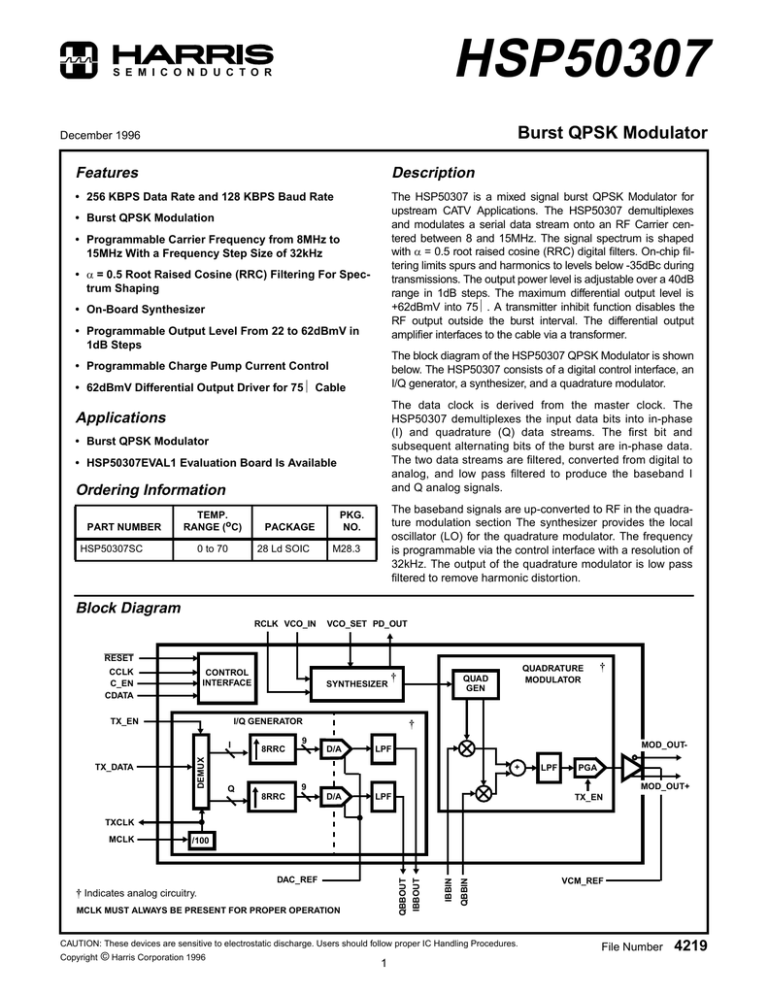
HSP50307 S E M I C O N D U C T O R Burst QPSK Modulator December 1996 Features Description • 256 KBPS Data Rate and 128 KBPS Baud Rate The HSP50307 is a mixed signal burst QPSK Modulator for upstream CATV Applications. The HSP50307 demultiplexes and modulates a serial data stream onto an RF Carrier centered between 8 and 15MHz. The signal spectrum is shaped with α = 0.5 root raised cosine (RRC) digital filters. On-chip filtering limits spurs and harmonics to levels below -35dBc during transmissions. The output power level is adjustable over a 40dB range in 1dB steps. The maximum differential output level is +62dBmV into 75Ω. A transmitter inhibit function disables the RF output outside the burst interval. The differential output amplifier interfaces to the cable via a transformer. • Burst QPSK Modulation • Programmable Carrier Frequency from 8MHz to 15MHz With a Frequency Step Size of 32kHz • α = 0.5 Root Raised Cosine (RRC) Filtering For Spectrum Shaping • On-Board Synthesizer • Programmable Output Level From 22 to 62dBmV in 1dB Steps The block diagram of the HSP50307 QPSK Modulator is shown below. The HSP50307 consists of a digital control interface, an I/Q generator, a synthesizer, and a quadrature modulator. • Programmable Charge Pump Current Control • 62dBmV Differential Output Driver for 75Ω Cable The data clock is derived from the master clock. The HSP50307 demultiplexes the input data bits into in-phase (I) and quadrature (Q) data streams. The first bit and subsequent alternating bits of the burst are in-phase data. The two data streams are filtered, converted from digital to analog, and low pass filtered to produce the baseband I and Q analog signals. Applications • Burst QPSK Modulator • HSP50307EVAL1 Evaluation Board Is Available Ordering Information PART NUMBER TEMP. RANGE (oC) HSP50307SC 0 to 70 PACKAGE 28 Ld SOIC The baseband signals are up-converted to RF in the quadrature modulation section The synthesizer provides the local oscillator (LO) for the quadrature modulator. The frequency is programmable via the control interface with a resolution of 32kHz. The output of the quadrature modulator is low pass filtered to remove harmonic distortion. PKG. NO. M28.3 Block Diagram RCLK VCO_IN VCO_SET PD_OUT RESET CCLK C_EN CDATA CONTROL INTERFACE TX_EN SYNTHESIZER † I/Q GENERATOR DEMUX I TX_DATA QUADRATURE MODULATOR QUAD GEN † 9 8RRC D/A MOD_OUT- LPF + Q † LPF PGA MOD_OUT+ 9 8RRC D/A LPF TX_EN TXCLK MCLK MUST ALWAYS BE PRESENT FOR PROPER OPERATION QBBIN QBBOUT DAC_REF † Indicates analog circuitry. IBBIN /100 IBBOUT MCLK CAUTION: These devices are sensitive to electrostatic discharge. Users should follow proper IC Handling Procedures. Copyright © Harris Corporation 1996 1 VCM_REF File Number 4219 HSP50307 Pinout 28 LEAD SOIC TOP VIEW MCLK 1 28 CCLK TXCLK 2 27 CDATA TX_EN 3 26 C_EN TX_DATA 4 25 DVCC RESET 5 24 RCLK DGND 6 23 AGND AVCC 7 22 PD_OUT AGND 8 21 VCO_IN 20 VCO_SET IBBOUT 9 19 AVCC QBBOUT 10 QBBIN 11 18 MOD_OUT- IBBIN 12 17 MOD_OUT+ DAC_REF 13 16 AVDD VCM_REF 14 15 AGND Pin Description SYMBOL TYPE DESCRIPTION MCLK I Master clock input (25.6MHz). (D) TXCLK O PSK data clock (256kHz) for PSK_DATA_IN. (D) TX_EN I Transmit enable. When high, the modulator output is enabled. This pin should be high for the entire burst. The signal is extended internally until data has fully exited the part before turning off for spurious free turn on and turn off. (D) TX_DATA I 256 KBPS serial data input. (D) RESET I Digital reset pin (active low). The part is reset immediately on assertion of the reset pin. The output of the part is disabled on the assertion of reset. The part will come out of reset 2 master clock periods after the reset is deasserted. Reprogramming (see Control Interface section) is needed after deassertion of reset for proper operation. (D) DGND I Negative supply for the digital filters and control. (P) AVCC I Positive supply for the quadrature modulator. AVCC should be tied to +5V analog. (P) AGND I Negative supply for the quadrature modulator. AGND is tied to GND. (P) IBBOUT O I baseband filtered output (A). QBBOUT O Q baseband filtered output. (A) QBBIN I Q baseband modulator input. (A) IBBIN I I baseband modulator input. (A) DAC_REF O D/A reference node. A 0.1µF capacitor to ground is suggested. (A) VCM_REF O Modulator common mode reference node. A 0.1µF capacitor to ground is suggested. (A) AGND I Negative supply for the cable interface. (P) AVDD I Positive supply for the cable interface (+9V analog). (P) MOD_OUT+ O Positive output drive pin for the cable interface. (A) MOD_OUT- O Negative output drive pin for the cable interface. (A) 2 HSP50307 Pin Description (Continued) SYMBOL TYPE DESCRIPTION AVCC I VCO_SET I/O VCO_IN I Voltage-controlled oscillator control voltage. (D) PD_OUT O Phase/frequency detector output. (D) AGND I Negative supply for the synthesizer. (P) RCLK I Synthesizer reference clock input (2.048MHz). (D) DVCC I Positive supply for the digital filters and control (+5V digital). (P) C_EN I Control interface enable for 3 wire interface. See Control Interface section. (D) CDATA I Serial data input for 3 wire interface. See Control Interface section. (D) CCLK I 3 wire interface clock. See Control Interface section. (D) Positive supply for the synthesizer (+5V analog). (P) VCO free running frequency set resistor (normally 6.25kΩ). (D) NOTE: (A) = analog, (D) = digital, (P) = power. Functional Description 0.8 0.7 The HSP50307 is designed to transmit 256 KBPS data using QPSK modulation on a programmable carrier over 75Ω cable lines. The incoming 256 KBPS data is first demultiplexed into in-phase (I) and quadrature (Q) data streams. The burst QPSK modulator shapes the two 128 KBPS demultiplexed data streams using interpolateby-8 root-raised cosine (RRC) filters with α = 0.5. The resulting 1.024MHz data streams are sent through D/A converters and are then sent through low-pass reconstruction filters for over 40dB image rejection. The baseband analog output and input pins allow the signals to be AC coupled. The returning analog signal is upconverted by an analog quadrature modulator. The control section is configured by loading 23 bits of information via a three-wire interface. These bits configure the DSP filter section, the carrier frequency, the analog synthesizer, and the output driver sections. COEFFICIENT VALUE 0.6 0.5 0.4 0.3 0.2 0.1 0 -0.1 -0.2 1 8 16 24 32 40 TAP NUMBER 48 56 64 FIGURE 1. NORMALIZED IMPULSE RESPONSE OF THE RRC INTERPOLATION FILTER WITH α = 0.5 Digital Filters REF -15.0 dBm # AT 60dB MKR 8.0960MHz -16.83dBm VBW 300Hz SPAN 400.0kHz SWP 13.3s PEAK LOG 5dB/ The burst QPSK modulator uses an interpolate-by-8 digital RRC filter on both the I and Q data streams. The shaping factor is set to α = 0.5. The FIR order of the digital RRC filter is 64. Figure 1 shows the impulse response of the RRC filter. Figure 2 is a spectrum analyzer plot of the modulator output for a baud rate of 128 kbaud and a pseudorandom data pattern. The 128kHz 3dB bandwidth and 192kHz stopband edges are readily apparent. WA SB SC FS CORR CENTER 8.0960MHz #RES BW 300Hz FIGURE 2. SPECTRUM OF 8.096MHz RANDOM DATA MODULATED CARRIER 3 HSP50307 Control Interface Synthesizer The QPSK modulator is configured via a serial three wire interface. When C_EN is high, 23 bits are shifted in at the CDATA pin on the falling edge of CCLK. Figure 3 shows the timing diagram for loading the serial configuration data. Table 1 describes the 23-bit serial configuration data. See the Synthesizer Section for more details on the frequency control bits. The synthesizer generates the quadrature LO’s for modulating the baseband data to RF. The carrier frequency is phase locked to the reference clock (RCLK). The carrier frequency, FC, has a frequency range of 8MHz to 15MHz with a resolution of 32kHz. Equation 1 gives the relationship between FC and the frequency of RCLK and the frequency control bits, M and A. TABLE 1. 23 BIT SERIAL DATA CONTROL INTERFACE DESCRIPTION 6(M + 1) + A F C = --------------------------------- F REF , 64 BIT POSITION FUNCTION (EQ. 1) where FREF equals the frequency of RCLK. Also, M and A can be determined by DESCRIPTION D0-D2 (Note) Synthesizer Control Bits Pre-scaler control register. A = (0 to 5), D2 is the MSB. D3-D9 Synthesizer Control Bits Feedback counter control register. M = (41 to 103) D9 is the MSB. D10 Synthesizer Enable Active high. This bit activates chip bias networks for normal operation. D10 = 0 places part in low power mode. D11 Charge Pump D11 = 0 sets charge pump current to Current 500µA. Control D11 = 1 sets charge pump current to 1mA. 64 A M + ---- = -----6 6 D12 Three-State Control D12 = 0 three-states the charge pump output when a pump up and down command occur simultaneously. D12 = 1 disables three-state. D13-D18 Attenuation Control Controls output power level. The binary value of the register corresponds to an attenuation amount. For example, 000100 corresponds to 4dB attenuation from the maximum 62dBmV level. D18 is the MSB. D19-D21 Reserved Used for test/diagnostic purposes. Set to 000. D22 DSP Shut Down Test mode; D22 = 0 sets the burst QPSK modulator in normal mode. D22 = 1 disables the digital filter. FC --------------- – 1. F REF (EQ. 2) “A” ranges from 0 to 5 and “M” ranges from 41 to 103. A and M are programmed via control bits D0-D2 and D3-D9, respectively. Values outside these ranges are invalid. I/Q Generator The I/Q Generator Section demultiplexes and time aligns the 256 KBPS input data into two data streams, I and Q. The first data bit following the assertion of the TX_EN signal is the I data of the first I/Q pair. Each I/Q pair determines the phase angle of the QPSK transmission signal. The relationship between I/Q pairs and phase angles is shown in Table 2. Since the QPSK encoding requires a pair of I and Q information to transmit one symbol, an even number of data bits must be provided for each burst. TABLE 2. QPSK ENCODING I Q PHASE 0 0 45o 0 1 135o 1 0 -45o 1 1 -135o NOTE: D0 is the first bit shifted into the part. TCCH CCLK TCDS TCDH C_DATA D22 D21 D20 D19 D3 D2 C_EN FIGURE 3. CONTROL INTERFACE TIMING DIAGRAM 4 D1 D0 HSP50307 Applications Example +5VDIGITAL 0.1µF 25.6MHz OSC DGND DATA SOURCE +5VANALOG 1 MCLK CCLK 28 2 TXCLK CDATA 27 3 TX_EN C_EN 26 4 TX_DATA DVCC 25 5 RESET RCLK 24 6 DGND AGND 23 7 AVCC PD_OUT 22 8 AGND VCO_IN 21 9 IBBOUT 10 QBBOUT CONTROL PROC. 2.048MHz OSC 2kΩ DGND 0.01µF +5VANALOG 100pF 6.25kΩ 0.1µF 0.01µF VCO_SET 20 AVCC 19 37.5Ω 0.1µF 11 QBBIN MOD_OUT- 18 12 IBBIN MOD_OUT+ 17 13 DAC_REF AVDD 16 14 VCM_REF AGND 15 CABLE TRANSFORMER RFOUT 0.1µF 0.1µF 37.5Ω 0.1µF +9VANALOG 0.1µF 0.1µF 0.1µF AGND AGND FIGURE 4. APPLICATIONS EXAMPLE OF THE HSP50307 applications example shown in Figure 4. It gives an overview of what is being accomplished but does not specify an exact carrier frequency or other programmable functions. These specifications are met given a valid control word combination and the applications circuit shown in Figure 4. Table 4 summarizes the performance of the applications example shown in Figure 4. Again, these specifications are met given a valid programmed mode. Figure 4 shows an applications example of the HSP50307. The MCLK source operates at 25.6MHz, and the RCLK operates at 2.048MHz. 0.1µF capacitors are connected from the IBBOUT to IBBIN and the QBBOUT to QBBIN, providing AC coupling to the analog upconverter section of the HSP50307. The control processor sends the 23-bit control word via the three-wire interface. The data source receives the 256kHz TXCLK from the HSP50307 and transmits data and enable signal at the 256kHz rate. NOTE: The HSP50307 is sensitive to layout. Users must make sure the input signals do not couple back into the output signals. The performance of the HSP50307 is also sensitive to the decoupling capacitors between 1) QBBOUT and QBBIN and 2) IBBOUT and IBBIN. The values shown in Figure 4 are recommended. The DAC_REF and VCM_REF are connected to 0.1µF capacitors to ground. Each of the differential drivers are loaded with a 37.5Ω resistor and a 0.1µF capacitor. The 37.5Ω resistors provide matching to the 75Ω cable. The capacitors perform AC coupling. The drive paths are sent to the cable transformer for data transmissions. Table 3 shows the general functional specifications for the 5 HSP50307 TABLE 3. GENERAL FUNCTIONAL SPECIFICATIONS AVCC, DVCC = +5V, AVDD = +9V; RCLK = 2.048MHz; MCLK = 25.6MHz; TA = 0oC To 70oC PARAMETER MIN TYP MAX UNIT 8.0 - 15 (Note) MHz QPSK Carrier Frequency Step Size - 32 - kHz Modulation Bandwidth - 192 - kHz Raised Cosine FIlter Response Excess Bandwidth (α) - 0.5 - - Transmit Level Adjust - 40 - dB Data Rate - 256 - KBPS Baud Rate - 128 - KBPS QPSK Carrier Frequency NOTE: May operate up to 20MHz. TABLE 4. QPSK PERFORMANCE SPECIFICATIONS AVCC, DVCC = +5V, AVDD = +9V; RCLK = 2.048MHz; MCLK = 25.6MHz; TA = 0oC to 70oC PARAMETER MIN TYP MAX UNITS Output Spurious Signals Less Than 54MHz - -40 -35 dBc Output Spurious Signals Greater Than 54MHz - -60 -50 dBc Off Mode Spurs - - -30 dBmV 59 62 65 dBmV Output Gain Adjust Relative Accuracy -0.5 0.2 0.5 dB Absolute Output Accuracy at Any Step -3.0 ±2 3.0 dB QPSK Carrier Phase Noise at 10kHz Offset - - -75 dBc/Hz QPSK Carrier Phase Noise at 1kHz Offset - - -60 dBc/Hz 35 40 - dBc QPSK I/Q Amplitude Imbalance - - 0.5 dB QPSK I/Q Phase Imbalance - - 2.0 Degree -0.3 - 0.3 dB Transmit Level (D18-D13 = 000000) QPSK Modulator Carrier Suppression QPSK Passband Amplitude Ripple 6 HSP50307 Absolute Maximum Ratings Thermal Information 5V Supply Voltage . . . . . . . . . . . . . . . . . . . . . . . . . . . . . . . . . . . 6.0V 9V Supply Voltage . . . . . . . . . . . . . . . . . . . . . . . . . . . . . . . . . . 11.0V ESD Classification . . . . . . . . . . . . . . . . . . . . . . . . . . . Class 1, HBM Thermal Resistance (Typical, Note 1) θJA (oC/W) SOIC Package . . . . . . . . . . . . . . . . . . . . . . . . . . . . . 70 Maximum Junction Temperature . . . . . . . . . . . . . . . . . . . . . . . 150oC Maximum Storage Temperature Range . . . . . . . . . .-65oC to 150oC Maximum Lead Temperature (Soldering 10s) . . . . . . . . . . . . . 300oC (SOIC - Lead Tips Only) Operating Conditions Temperature Range . . . . . . . . . . . . . . . . . . . . . . . . . . . .0oC to 70oC CAUTION: Stresses above those listed in “Absolute Maximum Ratings” may cause permanent damage to the device. This is a stress only rating and operation of the device at these or any other conditions above those indicated in the operational sections of this specification is not implied. NOTE: 1. θJA is measured with the component mounted on an evaluation PC board in free air. DC Electrical Specifications PARAMETER RCLK = 2.048MHz; MCLK = 25.6MHz; TA = 0oC to 70oC SYMBOL/PIN MIN TYP MAX UNIT 5V Supply Voltage AVCC, DVCC 4.75 5.0 5.25 V 9V Supply Voltage AVDD 8.55 9.0 9.45 V 5V Supply Current IAVCC, IDVCC - 55 - mADC 9V Supply Current IAVDD - 60 - mADC Logical One Input Voltage VIH 3.325 - - V Logical Zero Input Voltage VIL - - 1.575 V Output High Voltage VOH 2.6 - - V Output Low Voltage VOL - - 0.4 V AC Electrical Specifications PARAMETER AVCC, DVCC = +5V, AVDD = +9V; RCLK = 2.048MHz; MCLK = 25.6MHz; TA = 0oC to 70oC SYMBOL MIN TYP MAX UNIT RESET Pulse Width tRES 500 - - ns MCLK Period (25.6MHz) tMCP - 39.1 - ns RCLK Period (2.048MHz) tRCP - 488 - ns RCLK High tRCH 98 - - ns RCLK Low tRCL 98 - - ns CCLK Period (5MHz) tCCP 200 - - ns CCLK High tCCH 150 - - ns CCLK Low tCCL 150 - - ns CDATA Setup to CCLK tCDS 50 - - ns CDATA Hold from CCLK tCDH - - 50 ns C_EN Strobe Edge to CCLK tCES -100 - 100 ns TXCLK Period (256kHz) tDCP - 3910 - ns TXCLK High tDCH 195 - - ns 7 HSP50307 AC Electrical Specifications AVCC, DVCC = +5V, AVDD = +9V; RCLK = 2.048MHz; MCLK = 25.6MHz; TA = 0oC to 70oC (Continued) PARAMETER SYMBOL MIN TYP MAX UNIT TXCLK Low tDCL 195 - - ns TX_DATA Setup to TXCLK tDIS 150 - - ns TX_DATA Hold from TXCLK tDIH 0 - - ns Waveforms tMCP 1 2 tRCP MCLK tRCH tRCL PART IS ACTIVE AGAIN tRES RCLK RESET FIGURE 5. RESET AND MCLK WAVEFORMS FIGURE 6. RCLK WAVEFORM tCCP tCCL tCCH CCLK tCDS tDCP tCDH tDCL CDATA tDCH TXCLK tDIS C_EN tDIH TX_DATA tCES FIGURE 7. CONFIGURATION WAVEFORMS FIGURE 8. TRANSMIT DATA WAVEFORMS 8 HSP50307 Small Outline Plastic Packages (SOIC) M28.3 (JEDEC MS-013-AE ISSUE C) 28 LEAD WIDE BODY SMALL OUTLINE PLASTIC PACKAGE N INDEX AREA H 0.25(0.010) M B M INCHES E SYMBOL -B1 2 3 -C- e 0.25(0.010) M 0.1043 2.35 2.65 - 0.0118 0.10 0.30 - B 0.013 0.0200 0.33 0.51 9 C 0.0091 0.0125 0.23 0.32 - D 0.6969 0.7125 17.70 18.10 3 E 0.2914 0.2992 7.40 7.60 4 e C 0.10(0.004) C A M NOTES 0.0926 α A1 B MAX 0.0040 h x 45o A MIN A L D MILLIMETERS MAX A1 SEATING PLANE -A- MIN B S 0.05 BSC - 0.394 0.419 10.00 10.65 - h 0.01 0.029 0.25 0.75 5 L 0.016 0.050 0.40 1.27 6 8o 0o N α NOTES: 1.27 BSC H 28 0o 28 7 8o Rev. 0 12/93 1. Symbols are defined in the “MO Series Symbol List” in Section 2.2 of Publication Number 95. 2. Dimensioning and tolerancing per ANSI Y14.5M-1982. 3. Dimension “D” does not include mold flash, protrusions or gate burrs. Mold flash, protrusion and gate burrs shall not exceed 0.15mm (0.006 inch) per side. 4. Dimension “E” does not include interlead flash or protrusions. Interlead flash and protrusions shall not exceed 0.25mm (0.010 inch) per side. 5. The chamfer on the body is optional. If it is not present, a visual index feature must be located within the crosshatched area. 6. “L” is the length of terminal for soldering to a substrate. 7. “N” is the number of terminal positions. 8. Terminal numbers are shown for reference only. 9. The lead width “B”, as measured 0.36mm (0.014 inch) or greater above the seating plane, shall not exceed a maximum value of 0.61mm (0.024 inch) 10. Controlling dimension: MILLIMETER. Converted inch dimensions are not necessarily exact. All Harris Semiconductor products are manufactured, assembled and tested under ISO9000 quality systems certification. Harris Semiconductor products are sold by description only. Harris Semiconductor reserves the right to make changes in circuit design and/or specifications at any time without notice. Accordingly, the reader is cautioned to verify that data sheets are current before placing orders. Information furnished by Harris is believed to be accurate and reliable. However, no responsibility is assumed by Harris or its subsidiaries for its use; nor for any infringements of patents or other rights of third parties which may result from its use. No license is granted by implication or otherwise under any patent or patent rights of Harris or its subsidiaries. Sales Office Headquarters For general information regarding Harris Semiconductor and its products, call 1-800-4-HARRIS NORTH AMERICA Harris Semiconductor P. O. Box 883, Mail Stop 53-210 Melbourne, FL 32902 TEL: 1-800-442-7747 (407) 729-4984 FAX: (407) 729-5321 EUROPE Harris Semiconductor Mercure Center 100, Rue de la Fusee 1130 Brussels, Belgium TEL: (32) 2.724.2111 FAX: (32) 2.724.22.05 S E M I C O N D U C TO R 9 ASIA Harris Semiconductor PTE Ltd. No. 1 Tannery Road Cencon 1, #09-01 Singapore 1334 TEL: (65) 748-4200 FAX: (65) 748-0400
