Document 13771350
advertisement
High Precision 16-bit Readout Gas Sensor Interface in
0.13µm CMOS
Balaji Jayaraman and Navakanta Bhat
Department of Electrical Communication Engineering, Indian Institute of Science
Bangalore, India
Email: {jbalaji, navakant}@ece.iisc.ernet.in
based frequency-to-digital converter (FDC) suits this
purpose.
Abstract— A high precision 16-bit readout circuit for gas
sensor interface is realized in 0.13µm CMOS technology. The
front end signal conditioning circuit comprises a low power
resistance – to – time period converter with subthreshold
operation of transistors. The time-period proportional to the
transducer output is digitized using a counter based frequency
– to – digital conversion (FDC) technique. In order to handle
the sensor signal with a dynamic range of 160dB, subranging
technique is employed to provide feedback to front end circuit
interfacing the sensor. While the 3 MSBs of 16-bit word
restrict the input frequency to FDC between 1MHz and
10MHz, the 13-bit counter operates on this signal to provide a
worst case resolution of 0.4%. The power consumption of the
readout circuit is 366µW from a 1.2V supply.
There have been reports on resistive gas sensor interface
circuits [2],[4],[5]. In [2], a resistance – to – time period
converter is used as the FEC where the frequency output,
which is calibrated using a digital control, is readout through
an external microcontroller. A logarithmic converter forms
the FEC in [4]. Though this supports the wide dynamic
range, it loses out on high precision. In [5], a trans-resistance
amplifier followed by an ADC is used as the interface
circuit. This results in significant area and power overhead.
In this paper we report on a 16-bit readout gas sensor
interface realized in 0.13µm UMC technology, with 0.4%
resolution over a wide dynamic range of 160dB. FEC is
realized as resistance – to – time period converter with
subthreshold operation of transistors. The digital output is
obtained from an on-chip FDC employing subranging
technique. The circuit consumes 366µW.
I. INTRODUCTION
Integrated CMOS sensors offer several advantages such
as low cost, low power, small form factor, and high
reliability. Sensor signals typically have low signal
bandwidth (few Hz) [1], but may exhibit very wide dynamic
range [2],[3]. Front end signal conditioning circuitry (FEC)
must support the precision and dynamic range that is
expected of the sensors. It is convenient to have frequency or
time period of an RC relaxation oscillator as the analog
output signal from such sensors for better linearity and ease
of processing. The analog-to-digital conversion, which
enables further signal processing in the digital domain,
should not result in the degradation of the precision, but at
the same time, support the wide dynamic range. A counter
The paper is organized as follows. The design of FEC is
presented in section II. Section III deals with the FDC
design. Signal – to – noise ratio of the FDC is analyzed in
section IV. Concluding remarks are provided in section V.
II.
FEC ARCHITECTURE
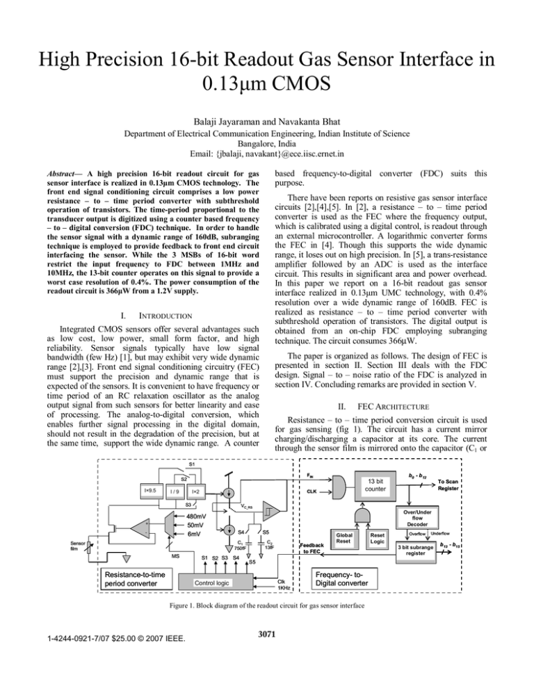
Resistance – to – time period conversion circuit is used
for gas sensing (fig 1). The circuit has a current mirror
charging/discharging a capacitor at its core. The current
through the sensor film is mirrored onto the capacitor (C1 or
S1
FIN
S2
I×9.5
I/9
I×2
CLK
S3
S5
S4
C2
13fF
S1 S2 S3 S4
Feedback
to FEC
Global
Reset
S5
Clk
1KHz
+
-
Control logic
Frequency- toDigital converter
Figure 1. Block diagram of the readout circuit for gas sensor interface
1-4244-0921-7/07 $25.00 © 2007 IEEE.
To Scan
Register
Over/Under
flow
Decoder
C1
750fF
Sensor
film
Resistance-to-time
period converter
b0 - b 12
VC_RS
480mV
50mV
6mV
MS
13 bit
counter
3071
Reset
Logic
Overflow
Underflow
3 bit subrange
register
b 13 - b15
C2). The current mirror operates for a large range of
resistance in the subthreshold region, leading to low power
consumption. The capacitor voltage is fed to a Schmitt
trigger, which controls the charging/discharging paths. The
resultant square wave output of the Schmitt trigger has its
time-period proportional to the sensor resistance. The sensor
resistance varies from 150Ω to 85MΩ with a resolution of
0.4% of the base value. Subranging technique is employed in
this case, limiting the frequency of the sensor circuit to a
band of 1MHz to 10MHz. The frequency feedback
information is provided by the digital readout of the FDC to
the control logic to select one of the three current scaling
paths, one of the two capacitors (13fF and 750fF), and one of
the three analog voltages (VR = 480mV, 50mV and 6mV)
such that the output frequency always lies in the designed
band. For stability considerations, a slight overlap is used in
the different bands.
The gas sensor readout circuit is shown in fig 2. The
current through the sensor film is given as Isensor = Vsensor Rsensor .
This current is mirrored onto the capacitor. Reverse body
bias of -1V is applied to the NMOS transistors in the current
mirror to enhance the subthreshold region. NMOS transistor
Subthreshold
operation
5.5nA – 55nA
Subthreshold
operation
50nA – 10µA
4.5µA – 45µA
(for 99.4% of
resistance range)
Voltage
reference
S3
Analog
Voltage
Sources
VBP1
S2
+
Output
S1
-
S2
S1
S4
C1
750fF
MS
Subthreshold
operation
Sensor
film
Control logic
Feedback
From FDC
Clk
1KHz
Cascode
transistor
Charge
pump
-1V
VBN1
-1V
50nA – 500nA
VBN2
100nA - 10µA
Clk
1MHz
Reverse
Body bias
Subthreshold operation
0.5µA - 5µA
Current foldback
C2
13fF
VBN3
Rsensor
Reverse
Body bias
MS -1V
S1
S2
S3
S4
S5
S5
(for 99.4% of resistance range)
in current mirror operates in subthreshold region over 99.4%
of the entire resistance range. Cascode transistors are used to
increase the output impedance. The current through the
capacitor C is given as I c = C ∆V ∆T where ∆V is the
change in voltage across the capacitor, which is set by the
Schmitt trigger threshold voltages (0.3V and 0.9V). ∆T is
half the time-period of the Schmitt trigger output. Ic is
limited to the range of 100nA to 10µA. As shown in fig 2,
once the Isensor crosses this band, the current is folded back to
the designed band using the two current mirror circuits. S1,
S2 and S3 are mutually exclusive switches, with S3 initially
on. As shown in fig 2(a) and 2(b), if Ic exceeds 10µA, then
S2 is turned on. Conversely, if Ic falls below 100nA, S1 is
turned on. S5 and S4 are on for Ic ranges of 100nA to 1µA,
and 1µA to 10µA respectively. The switches MS are
simultaneously operated to set an appropriate VR so that the
output frequency always lies in the designed band.
III.
FDC ARCHITECTURE
The frequency output of FEC is digitized by the FDC
block. The 16-bit FDC is implemented with 3 MSBs
providing the subrange information and the 13 LSBs of the
counter providing the required resolution (fig 1). The 13-bit
synchronous counter is constructed with a clock frequency of
1KHz. Since the signal bandwidth (i.e. the rate of change of
the input signal frequency) is low (few hundreds of mHz to a
few Hz), a reference clock of 1KHz is acceptable. This
corresponds to a worst case resolution of 0.2% (excluding
the one-cycle count error). Whenever 13-bit counter
overflows (underflows), the subrange register is incremented
(decremented). Thus the 3-bit subrange register will take
every decade range of frequencies and fold it back to a range
between 1MHz and 10MHz, by providing feedback to FEC.
Fig 3. shows the control logic, which is implemented as a
finite state machine, running on 1KHz clock. The subrange
register bits are fed to two combinational logic blocks - an
incrementer and a decrementer. Based on the overflow/
underflow information, outputs of one of the blocks form the
D-inputs to the subrange register. If there is neither overflow
-5
Current ( A )
10
-6
10
Mirrrored and
folded back
Mirrrored and
folded back
S2 ON
S3 ON
S1 ON
-7
10
-9
10
-8
10
-7
10
-6
10
-5
10
Current through the sensor film ( A )
-4
10
Figure 3. Control logic for the FEC signal conditioning.
Figure 2. (a) Gas sensor readout circuit. (b) Mirrored and folded back
current from the three scaling paths.
3072
S4 ON
S5 ON
V = 480mV
Digital output
S2 0N
S3 ON
S1 ON
V = 6mV
V = 50mV
R
R
R
Overflow /
Underflow
decoder
FEC
3-bit subrange register
3
10
Control logic for FEC signal
conditioning
500
SB = 010 SB = 001 SB = 000 SB = 101 SB = 100 SB = 011
-8
10
-7
10
-6
10
-5
10
-4
10
-3
10
Conductance of the sensor film ( 1 / ohms )
-2
10
Resistance-to-Time period
Converter
Figure 4. Digital code versus the conductance of the sensor film
nor underflow, then the present outputs (Q) are fedback as
D-inputs. Thus the same state will be retained till there is
either an underflow or an overflow. The combinational logic
for the control switches is obtained from the D-inputs of the
register.
The digital output, showing the subranging, is plotted
against the conductance of the sensor film in fig 4. The
maximum DNL is ±1LSB (1 LSB corresponds to 2KHz).
This is due to the one cycle count error. The integral
nonlinearity (INL) is observed to be ± 1 LSB (in a subrange).
Thus the FDC provides a worst case resolution of 0.4% over
the resistance range of 150Ω to 85MΩ, corresponding to
163dB dynamic range (20log10 (85M/(0.4% of 150)) =
163dB).
Fig 5 shows the micrograph of the chip realized in
0.13µm CMOS 1P8M technology. The total area consumed
(FEC + FDC) is 30215µm2. The power consumption is
366µW from a 1.2V supply.
IV.
Circuit for 1-bit
counter
FDC
5000
SIGNAL TO NOISE AND DISTORTION RATIO (SNDR)
The input signal range to FDC is from 1MHz to 10MHz
(in a subrange). The resolution or step size in this band is
Figure 5. Chip micrograph with layout details of FEC and FDC. The
chip has 8 readout channels for interfacing with a sensor array.
4KHz. Considering only the quantization noise, the signal to
noise ratio is given as
2
9M
2 2
SNR = 10 log 10
= 68.8 dB
(4 K )2
12
The effective number of bits (ENOB) is calculated to be
14.13 bits for the 16-bit FDC.
MATLAB simulations were performed to validate the
above result. The input signal is a pulse waveform whose
frequency varies by 0.5MHz about the mean value of
1.5MHz at the rate of 50 Hz. Mathematically, the frequency
of the pulse waveform is given as
f in = (1.5 MHz) + (0.5 MHz) sin (2π . 50. t )
TABLE I
PERFORMANCE COMPARISON OF RECENT RESISTANCE READOUT CIRCUITS
Value
Parameter
Sensing scheme
Input range
Dynamic range
Supply voltage
Power dissipation
Area Consumed
CMOS Technology
(1)
This work
M.Malfatti et al 2006
[2]
D.Barrettino et al 2004
[4]
M.Grassi et al. 2005
[5]
R Æ T conversion
R Æ T conversion
150Ω – 85MΩ
163 dB
1.2V
326µW
12000µm2
0.13µm
500KΩ – 1GΩ
115dB
3.3V
3.1mW
0.35µm
(Log R) Æ V
conversion
1KΩ - 10MΩ
5V
0.8µm
R Æ V conversion +
ADC
100Ω - 10MΩ
3.3V
< 5mW
1.625mm2
0.35µm
3073
(2)
TABLE II
PERFORMANCE AND COMPARISON OF RECENT TIME-TO-DIGITAL CONVERTERS
Value
Parameter
Input range
Dynamic range
Precision
No. of bits
DNL
INL
Estimated SNDR
SFDR
Estimated ENOB
Supply voltage
Power dissipation
Refresh time
Area Consumed
This work
P. Chen et al. 2005 [1]
150Ω - 85MΩ (converted to
time : 0.1µs - 1µs)
163dB
4KHz in 1MHz – 10 MHz
band
16-bit
±1 LSB (2KHz)
±1 LSB (2KHz)
68.8 dB (in a subrange)
> 55.85 dB
14.13
1.2V
40µW
1ms
18215µm2
00C - 1000C
(converted to time)
55. 91dB
0.160C
0.13µm
CMOS Technology
K.Karadamoglou et al.
2004 [6]
C.Hwang et al 2004
[7]
E.R.Ruotsalainen et
al. 2000 [8]
50 ps - 2.048µs
-
10ns – 2.5 µs
92.2 dB
50ps – 1ns
-
97.86dB
32ps
10-bit
3.3V
490µW
1ms
0.175mm2
11-bit
±1 LSB
5V
< 10mW
-
± 0.55 LSB
+1 to -1.5 LSB
3.3V
< 50mW
0.6mm2
0.35µm
0.8µm
0.35µm
± 0.156 LSB
5V
350mW
< 6.3 µs
11.9mm2 (including
pads)
0.8µm
The counter output data is collected at the rate of 1KHz.
1K points are collected for FFT computation. Equation (1) is
valid under the condition that the time resolution is infinite.
The computation time increases exponentially with the
increase in time resolution. Hence, in Matlab, input sampling
frequency of 150MHz was used, corresponding to time step
of 6.67ns. This discretization in time leads to clipping of the
signal at higher frequencies leading to a saturated count
value. This results in harmonic distortion. It is observed that
both SNDR and Spurious Free Dynamic Range (SFDR)
improve with the increase in sampling rate used in Matlab.
The SNDR obtained for 1MHz swing is 46.1dB and the
SFDR obtained is 55.85dB. The SNDR for full scale input
(9MHz amplitude) is calculated to be 65dB. It is expected
that with further increase in the sampling rate, the SNDR
would approach the ideal value of 68.8dB. The chip testing is
under progress to validate this.
The performance of the designed FEC (obtained through
SPICE simulations) is benchmarked against some of the
recent reports in the literature (Table I). There is a significant
reduction in power consumption due to subthreshold
operation of transistors. Considering the power and area
metrics, the FDC performance is superior to other published
reports, as seen in Table II.
also be used in low power, low bandwidth, wide dynamic
range and high precision sensor applications.
REFERENCES
[1]
[2]
[3]
[4]
[5]
[6]
V.
CONCLUSION
The design and implementation of readout circuit with a
dynamic range of 160dB is presented for gas sensor
interface. The subthreshold operation of the transistors in the
front end signal conditioning circuit results in a low power
implementation. Subranging technique is employed to cover
the wide dynamic range with high linearity. The 16-bit FDC
has an accuracy of 0.4% in the subrange of 1MHz – 10MHz.
ENOB is estimated to be 14.13 bits. The designed FDC can
[7]
[8]
3074
Poki Chen, Chun-Chi Chen, Chin-Chung Tsai, and Wen-Fu Lu, “A
time-to-digital converter based CMOS smart temperature sensor,”
IEEE J. Solid-State Circuits, vol. 40, No. 8, pp. 1642 – 1648, August
2005.
M.Malfatti, M.Perenzoni, N.Viarani, A.Simoni, L.Lorenzelli, and
A.Baschirotto, “A complete front-end system readout and temperature control for resistive gas sensor array,” Proc. of the 2005 European Conf. on Circuit Theory and Design, vol.3, pp. 31-34, 2005.
R.Rankinen, K. Maatta, and J. Kostamovaara, “Time-to-digital
conversion with 10 ps single shot resolution,” 6th Mediterranean
Electrotechnical Conference Proceedings, vol. 1, pp. 319 – 322,
1991.
Diego Barrettino, Markus Graf, Wan Ho Song, Kay-Uwe Kirstein,
Andreas Hierlemann, and Henry Baltes, “Hotplate-based monolithic
CMOS microsystems for gas detection and material characterization
for operating temperatures up to 500oC,” IEEE J.Solid-State Circuits,
vol. 39, No.7, pp. 1202 – 1207, July 2004.
M.Grassi, P.Malcovati, and A.Baschirotto, “Flexible high-accuracy
wide-range gas sensor interface for portable environmental nosing
purpose,” IEEE International Symposium on Circuits and Systems,
vol. 6, pp. 5385-5388, May 2005.
Kostas Karadamoglou, Nikolaos P. Paschalidis, Emmanuel Sarris,
Nikos Stamatopoulos, George Kottaras, and Vassilis Paschalidis, “An
11-bit high-resolution and adjustable-range CMOS time-to-digital
converter for space science instruments,” IEEE J. Solid-State
Circuits, vol. 39, No. 1, pp. 214 – 222, January 2004.
Chorng-Sii Hwang, Poki Chen, and Hen-Wai Tsao, “A high precision
time-to-digital converter using a two level conversion scheme,” IEEE
Trans. on Nuclear Science, vol. 51, No. 4, pp. 1349 – 1352, August
2004.
Elvi Raisanen-Ruotsalainen, Timo Rahknonen, and Juha
Kosamovaara, “An integrated time-to-digital converter with 30-ps
single shot resolution,” IEEE J. Solid State Circuits, vol. 35, No.10,
pp. 1507– 1510, October 2000.
