Compositional dependence properties change in S Se Sb alloys
advertisement
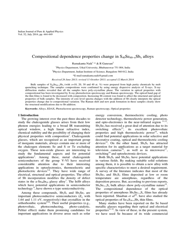
Indian Journal of Pure & Applied Physics Vol. 52, July 2014, pp. 444-449 Compositional dependence properties change in S40Se60−xSbx alloys Ramakanta Naik1, * & R Ganesan2 1 2 Physics Department, Utkal University, Bhubaneswar 751 004, India Physics Department, Indian Institute of Science, Bangalore 560 012, India *E-mail:ramakanta.naik@gmail.com Received 26 June 2013; revised 11 October 2013; accepted 12 March 2014 Bulk samples of S40Se60−xSbx (with x=10, 20, 30 and 40 at. %) were prepared from high purity chemicals by melt quenching technique. The samples compositions were confirmed by using energy dispersive analysis of X-rays. X-ray diffraction studies revealed that all the samples have poly-crystalline phase. The variation in optical properties with compositional has been investigated by X-ray photoelectron spectroscopy and Raman spectroscopy. The optical band gap of the thin films is found to be decreased with composition. Increasing Sb content was found to affect the structural and optical properties of bulk samples. The intensity of core level spectra changes with the addition of Sb clearly interprets the optical properties change due to compositional variation. The Raman shift and new peak formation in these samples clearly show the structural modifications due to Sb addition. Keywords: Alloys, EDAX, Photoelectron spectroscopy, Raman spectroscopy, Optical properties 1 Introduction The growing interest over the past three decades to study the chalcogenide glasses arises from their low phonon energies leading to a broad IR transmitting optical window, a high linear refractive index, chemical stability and the possibility of changing their physical properties with composition1. Chalcogenide glasses, which are recognised as an important group of inorganic materials, always contain one or more of the chalcogen elements Se and S or Te excluding oxygen. These non-oxide glasses are interesting to study the fundamental aspects and for potential applications2. Among these, metal chalcogenide semiconductors of the group V-VI have received considerable attention due to their interesting applications in optoelectronics, thermoelectric and photoelectric devices3-6. They have wide range of electrical, structural and optical properties. The effect of Sb incorporation modifies the density of defect states in the a-Se90In10 glassy alloy7. The InSb alloys which have potential applications in semiconductor technology 8, have shown n type semiconductivity. Among these compounds, Sb2S3 and Sb2Se3 are important photoconductive semiconductors (Eg with 1.64 and 1.11 eV, respectively) that crystallize in the orthorhombic system9,10. Their useful properties (e.g., photovoltaic, photoconducting, photo-catalytic, Peltier effect) make them promising candidates for important applications in diverse areas such as solar energy conversion, thermoelectric cooling, photo detector technology, thermoelectric power generation, and opto-electronics in the near-infrared region 11,12. Sb2Se3 has received a great deal of attention due to its switching effects13, its excellent photovoltaic properties and high thermoelectric power14, which could find potential applications in solar selective and decorative coating, optical and thermoelectric cooling devices15. On the other hand, Sb2S3 has attracted attention for its applications as a target material for television cameras16, as well as in microwave17, switching18 and optoelectronic devices. Both Sb2S3 and Sb2Se3 have potential applications in various fields. By making suitable solid solutions among them, it is possible to obtain a new alloy with specific characteristics to meet a desired requirement. A survey of the literature indicates that most of the Sb2Se3 and Sb2S3 films deposited at low or room temperature are amorphous, regardless of the deposition process. But, according to previous reports, Sb2Se3−xSx bulk alloys show poly-crystalline nature19. The compositional dependence of the optical properties of amorphous Sb2Se3−xSx films has already been reported. Shaaban et al20. have also studied the optical properties of Se70S30−xSbx thin films. Many studies have been reported on the Se based metallic glasses regarding their optical and electrical properties21-32. In view of these, in the present system, we have used Se because of its wide commercial 445 NAIK & GANESAN: PROPERTIES CHANGE IN S40Se60−xSbx ALLOYS applications. Its device applications like switching, memory and xerography etc. made it attractive. It also exhibits33 a unique property of reversible transformation. This property makes it very useful in optical memory devices. But in pure state it has disadvantages because of its short lifetime and low sensitivity. To overcome these difficulties, certain additives are used for getting various properties like greater hardness, higher sensitivity, higher crystallization temperature, higher conductivity and smaller ageing effects as compared to pure amorphous34 Se. Here, we have chosen S as an additive to overcome these problems. In the present system, Sb is incorporated in the Se–S system. The addition of third element creates compositional and configurationally disorder in the system. In the present paper, the optical properties of amorphous semiconductor S40Se60−xSbx bulk alloys with x=10, 20, 30 and 40 at. % prepared by melt quenching technique have been studied. The thin films prepared from these alloys have been studied to investigate the change in optical band gap. 2 Experimental Details Bulk glassy S40Se60−xSbx samples with a wide range of composition (x=10, 20, 30 and 40 at. %) were prepared from pure elements of Se, S and Sb (5N, Aldrich and Sigma Chemical Co.) using the meltquench technique. Stoichiometric amounts of highpurity elements were weighed and placed into a precleaned silica tube. The tube was then sealed under vacuum at a pressure of about 5×10⁻⁶ Pa. The silica ampoules were placed in a programmable rocking furnace and slowly heated up to 950°C with a temperature ramp of about 10°C/min. In order to ensure proper mixing and homogeneity, the samples were kept at 950°C for about 24 h with continuous gentle rocking. After full homogenisation of the melt, the ampoules were rapidly quenched to room temperature in ice water. The ampoules were carefully broken to get the sample pieces. Though the samples were cut in the open air, the chance of oxide formation (Sb2O3) is very less as the sample is already formed the different phases. The elemental compositions of these alloys were checked by energy dispersive X-ray analysis (EDAX) in Sirion XL 40 in which EDAX is attached. The scan was done at 20 kV with 40 µA emission current exposing a sample of 1 cm2 size at 2×10⁻⁵ Pa pressure and the estimated average precision was less than 3% in atomic fraction in each element which is presented in Table 1 and shown in Fig. 1. The polycrystalline state of the alloys were checked by X-ray (Philips, CuKα, λ=1.54 Å) Diffractometer (XRD). The presence of both amorphous peak and crystalline peaks confirms polycrystalline state of the prepared samples which are shown in Fig. 2. The XPS core level band spectra were obtained with monochromatic Al KĮ X-rays (1486.6 eV) at a vacuum of 10−7 Pa in Multilab 2000 Thermo Scientific UK instrument. The XPS data consisted of survey scans over the entire binding energy (BE) and selected scans over the core level peaks of interest. An energy increment of 1 eV was used for recording the survey spectra and 0.05 eV for the case of core level spectra. The core level peaks were recorded by sweeping the retarding field and using the constant pass energy of 30 eV. The data were averaged over three scans. The reproducibility of the measurements was checked on different regions of the investigated surfaces. For insulators such as glasses, the charging effect can change the BE of the electrons from sample to sample. Hence, the measurement of the absolute BE of electrons from a specified energy level is not reliable. The C 1s line from either adventitious carbon or intentionally added graphite powder on the surface has been widely used for charge referencing35,36. For this study, the adventitious carbon was used as a reference and the BE of the reference C 1s line was set as 284.6 eV. For each sample, a calibration factor was calculated from the difference between the measured C 1s BE and the reference37 value 284.6 eV. The original BE data were corrected according to the calibration factor. The room temperature Raman spectra were recorded in the Table 1 — Measured elemental composition from EDAX for S40Se60−xSbx samples with x=10, 20, 30 and 40 at. % x=10 SK Sb L Se K Total x=20 x=30 x=40 Observed Calculated Observed Calculated Observed Calculated Observed Calculated 39.59 9.38 51.03 100.00 40 10 50 100.00 39.42 19.46 41.12 100.00 40 20 40 100.00 38.96 29.16 33.88 100.00 40 30 30 100.00 39.78 39.53 20.69 100.00 40 40 20 100.00 446 INDIAN J PURE & APPL PHYS, VOL 52, JULY 2014 Fig. 2 — XRD patterns of the S40Se60-xSbx samples with x=10, 20, 30 and 40 at. % The thin films of thickness 800 nm were prepared from the bulk samples by thermal evaporation technique. The room temperature transmission spectra were recorded by using the Fourier Transform Infrared (FTIR) spectrometer (Bruker Optics (IFS66v/S) in the visible wavelength range 500-1100 nm. Fig. 1 — EDAX spectrum of the S40Se60-xSbx samples with (a) x=10, (b) 20, (c) 30 and (d) 40 at. % 180° backscattering geometry, using a 532 nm excitation from a diode pumped frequency doubled Nd-YAG solid state laser and a custom built Raman spectrometer equipped with SPEX TRIAX 550 monochromator and a liquid nitrogen cooled CCD. Laser power at the sample was ~15 mW and a typical spectrum acquisition took ~ 1-2 min. 3 Results and Discussion The composition analysis of S40Se60−xSbx samples with x = 10, 20, 30, and 40 at. % confirms the presence of antimony, selenium and sulphur in the prepared bulk samples. From the obtained results, it is revealed that the alloys with indicated x were deficient in Sb and S. But, contained a slight excess of Se consequently revealing a nearly stoichiometric compositions (see Table 1). Figure 1 shows the EDAX spectrum of S40Se60-xSbx material in bulk form as representative spectrum. One can observe the increased peak intensity for Sb whereas a decrease in for Se with Sb addition. The XRD patterns shown in Fig. 2 reveals that the prepared samples are polycrystalline in nature and the sharp peaks shown represent the different planes of the crystal structures. The oxygen effect is seen in the XPS spectra which gives O1s core level peak. This surface oxides forms little amount of Sb2O3 on the sample surface which has little effect on the optical band gap. The signature of the O1s peak is very less as shown in Fig. 3. But, as all the samples were handled in the same atmospheric condition. So, the effect is normalized. The XPS spectra in Fig. 4 clearly show the compositional dependence spectra change due to Sb addition. The Sb 4d peak (at 33 eV) intensity gradually increases with addition of Sb into S40Se60−xSbx. Similarly, Se 3d peak (at 55 eV) NAIK & GANESAN: PROPERTIES CHANGE IN S40Se60−xSbx ALLOYS 447 Fig. 5 — XPS core level spectra of Se 3p and S 2p of the S40Se60−xSbx samples with x=10, 20, 30 and 40 at. % Fig. 3 — XPS core level spectra of O 1s and Sb 3d peak Fig. 4 — XPS core level spectra of Sb 4d and Se 3d of the S40Se60xSbx samples with x=10, 20, 30 and 40 at. % intensity decreases with the incorporation of Sb. The Se vacancy is being filled up by Sb atoms. The peak at Sb 4d peak slightly moves towards higher binding energy side. This may be due to the formation of more no of Sb-Sb homopolar bonds as the Sb % increases. The Se 3d peak shifts from 55.13 eV (Sb 10%) to 54 eV (Sb 40%) due to the formation of Sb-Se bonds. This is because the electro negativity of Se (2.55) is more than that of Sb (2.08). As the S % remains constant in all the compositions, the S 2p peak intensity should remain the same. But, the EDAX data show that there are little variations in the chemical compositions. The Se 3p3 (161.7 eV), S 2p (162.6 eV) and Se 3p1 (167.3 eV) peaks are very close to each other and we cannot distinguish S 2p peak from Se 3p3 peak (Fig. 5). So, the intensity variations with Sb addition clearly reflect the compositional dependence XPS core level change. Fig. 6 — Raman spectra of the S40Se60-xSbx samples with x=10, 20, 30 and 40 at. % Direct evidence of structural changes in S40Se60−xSbx samples caused by addition of Sb was obtained from Raman spectra (Fig. 6). According to the molecular model38, each Sb atom in the S-Sb-Se ternary alloys is covalently bonded to three Se atoms in a pyramidal unit (Sb-Se3), and Sb atoms are covalently bonded to three S atoms in a pyramidal unit (Sb-S3). The basic structural units SbSe3 and SbS3 are interconnected through bridging S atoms. The coupling between the basic structural groups via S atoms is assumed to be weak, and the vibrational modes are separated into SbS3 and SbSe3 like modes. The S40Se60−xSbx samples have an over stoichiometry of metal atoms (Sb), and some Sb-Sb bonds should be present in the alloy too. The SbS3 pyramidal vibrational band is developed at 302 cm−1 in the neighborhood of the dominant vibrational band of SbSe3 at 249 cm-1 in the Raman spectra. Initially, there was a small peak at 303 cm−1 and 249 cm−1 in INDIAN J PURE & APPL PHYS, VOL 52, JULY 2014 448 (Eg). It is found that the optical band gap decreases from Eg = 2.01 eV for Sb 10 % to Eg = 1.68 eV for Sb 40% as the absorption edge shifts to lower photon energies as the Sb content increases (Fig. 7). The Tauc′s model40 based on the electronic transitions between the localized states in the band edge tails may be well valid for such systems. The decrease in Eg in the amorphous films can be explained by the increased tailing of the band tails in the gap41. The addition of Sb creates localized states in the band gap. This variation in optical band gap well supports the observed changes in the bulk alloys. Fig. 7 — Band gap variation with composition the spectrum as shown in Fig. 5, but as Sb % increases, both the peak becomes prominent. It is clear that the band at 302 cm−1 is due to the Sb-S vibration in Sb-S3, (S2) Sb-Sb (S2) and the band at 249 cm−1 is due to the Sb-Se vibration in Sb-Se3, (Se2) Sb-Sb (Se2). The peak at 118 cm−1 corresponds to disulphide bonds S-S (or two membered S2 chains) in S2Sb-S-S-SbS2 vibration. The peak at position 450 cm−1 in the spectra may be due to formation of S-S bonds. There is a small shift in the peak at 249 cm−1 which moves towards the lower wave number as Sb % increases which indicates the structural changes occurring in the system. The peak at 190 cm−1 corresponds to diselenide bonds Se-Se (or two membered Se2 chains) in Se2Sb-Se-Se-SbSe2 vibration. The peak intensity gradually decreases with addition of Sb and extra peak develops at around 198 cm−1 corresponds to the formation of Sb2Se3. The new vibrational peaks developed and slight shift in the wave number clearly indicates the structural modification occurring in the system. The optical band gap of the prepared films has been calculated by the equation: (αhν)1/2=B1/2(hν − Eg) …(1) where B is the Tauc parameter that depends upon the transition probability and Eg is the optical band gap of the film. The region with high absorption is characterized with interband transitions between valence band and conduction bands. By plotting (αhν)1/2 versus hυ, the slope of the straight line fitting gives the value of B while the intercept of the straight line to hν axis gives the value of optical band39gap 4 Conclusions The compositional dependence of S40Se60-xSbx samples with x = 10, 20, 30, and 40 at. % was studied through EDAX, XPS and Raman spectroscopy. The EDAX data showed the observed composition with homogeneity after the alloy preparation. The bulk alloys are found to be polycrystalline in nature. The structural modifications occurred with Sb addition was confirmed from the Raman study. The XPS core level spectra change supports the compositional and structural modifications. The optical band gap decreases with increase in Sb shows the creation of localised states in the gap. Acknowledgement The authors thank Department of Science and Technology (DST), Govt of India for DST-INSPIRE Research grant and using the National Facility for Optical Spectrometry at Department of Physics and Surface Science facility, Indian Institute of Science (IISc) for XPS measurement. References 1 Savage J A, Infrared Optical Materials & their Antireflection Coatings, Adam Hilger, Bristol, (1985). 2 Sunandana C S, Indian J Pure & Appl Phys, 46 (2008) 7. 3 Chokalingam M J, Rao K N, Rangarajan R & Suryanarayana C V, J Phys D Appl Phys, 3 (1970) 1641. 4 Montrimass E & Pazera A, Thin Solid Films, 34 (1976) 1641. 5 Roy B, Chakraborty B R, Bhattacharya R & Dutta A K, Solid State Commun, 25 (1978) 617. 6 Bhattacharya R N & Pramanik P, Sol Energy Mater, 6 (1982) 317. 7 Shukla S, Singh S P & Kumar S, Indian J Pure & Appl Phys, 49 (2011) 545. 8 Viswakarma S R, Verma A K, Tripathi R S N & Das S, Indian J Pure & Appl Phys, 50 (2012) 339. 9 Zheng X W, Xie Y, Zhu L Y, Jiang X C, Jia Y B & Sun Y P, Inorg Chem, 41 (2002) 455. 10 Yu Y, Wang R H, Chen Q & Peng L, J Phys Chem B, 110 (2006) 13415. NAIK & GANESAN: PROPERTIES CHANGE IN S40Se60−xSbx ALLOYS 11 Rajapure K, Lokhande C & Bhosele C, Thin Solid Films, 311 (1997) 114. 12 Kim I, Mater Lett, 43 (2000) 221. 13 Black J, Conwell E M, Sigle L & Spencer C W, J Phys Chem Solids, 2 (1957) 240. 14 Platakis N S & Gatos H C, Phys Status Solidi A Appl Res, 13 (1972) 1. 15 Rajapure K Y, Lokhande C D & Bhosele C H, Thin Solid Films, 311 (1997) 114. 16 Ghosh C & Varma B P, Thin Solid Films, 60 (1979) 61. 17 Grigas J, Meshkauskas J & Orliukas A, Phys Status Solidi A Appl Res, 37 (1976) 39. 18 Ablova M S, Andreev A A, Dedegkaev T T, Melekh B T, Pevtsov A B, Shendel N S & Shumilova L N, Sov Phys Semicond, 10 (1976) 629. 19 El-Sayad E A, J Non-Cryst Solids, 354 (2008) 3806. 20 Shaaban E R, El-Hagary M, Emam-Ismail M & El-Den M B, Philos Magazine, 91 (2011) 1679. 21 Hosni H M, Fayek S A, El-Sayed S M, Roushdy M & Soliman M A, Vacuum, 81 (2006) 54. 22 Soltan A S, Abu EL-Oyoun M & Abdel-Latief A Y, Mater Chem Phys, 82 (2003) 101. 23 Khan S A, Zulfequar M, Khan Z H & Husain M, Opt Mater, 20 (2002) 189. 24 Ahmad A, Khan S A, Sinha K, Kumar L, Khan Z H, Zulfequar M & Husain M, Vacuum, 82 (2008) 608. 25 Bhuiyan M R A, Saha D K & Firoj Hasan S M, Indian J Pure & Appl Phys, 47 (2009) 787. 449 26 Majeed Khan M A, Kumar S, Husain M & Zulfequar M, Mater Lett, 62 (2008) 1572. 27 El-Kabnay N, Shaaban E R & Abou-Sehly A M, Phys B Condens Matter, 403 (2008) 31. 28 Thakur A, Singh G, Saini G S S, Goyal N & Tripathi S K, Opt Mater, 30 (2007) 565. 29 Sharma P & Katyal S C, Thin Solid Films, 515 (2007) 7966. 30 Bhuiyan M R A, Saha D K & Firoj Hasan S M, Indian J Pure & Appl Phys, 49 (2011) 180. 31 Hafiz M M, Othman A A & Al-Motasem A T, Phys B Condens Matter, 390 (2007) 348. 32 Majeed Khan M A, Zulfequar M & Husain M, Opt Mater, 22 (2003) 21. 33 Tanka K, Phys Rev B, 39 (1989) 1270. 34 Srivastava S K, Dwivedi P K & Kumar A, Physica B, 183 (1993) 409. 35 Moulder J F, Sticker W F, Sobol P E & Bomben K D, Hand Book of X-Ray Photoelectron Spectroscopy, Perkin Elmer, Eden Pairie, MN, (1992). 36 Stec W J, Morgan W E, Albridge R G & Van Wazer J R, Inorg Chem, 11 (1972) 219. 37 Barr T L & Seal S, J Vac Sci Technol A, 13 (1995) 1239. 38 Lucovsky G & Martin R M, J Non Cryst Solids, 8 (1972) 185. 39 Naik R, Ganesan R & Sangunni K S, Thin Solid Films, 518 (2010) 5437. 40 Tauc J, The Optical Properties of Solids, North Holland, Amsterdam, (1970) 227. 41 Nagel P P, Tichy L, Triska A & Ticha H, J Non-Cryst Solids, 59 (1983) 1015.

