Comparison of OpAmp Based and Comparator Based Switched Capacitor Filter Manodipan Sahoo
advertisement
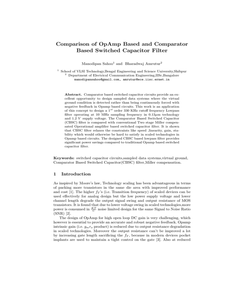
Comparison of OpAmp Based and Comparator Based Switched Capacitor Filter Manodipan Sahoo1 and Bharadwaj Amrutur2 1 School of VLSI Technology,Bengal Engineering and Science University,Shibpur 2 Department of Electrical Communication Engineering,IISc,Bangalore manodipansahoo@gmail.com, amrutur@ece.iisc.ernet.in Abstract. Comparator based switched capacitor circuits provide an excellent opportunity to design sampled data systems where the virtual ground condition is detected rather than being continuously forced with negative feedback in Opamp based circuits. This work is an application of this concept to design a 1st order 330 KHz cutoff frequency Lowpass filter operating at 10 MHz sampling frequency in 0.13µm technology and 1.2 V supply voltage. The Comparator Based Switched Capacitor (CBSC) filter is compared with conventional Two stage Miller compensated Operational amplifier based switched capacitor filter. It is shown that CBSC filter relaxes the constraints like speed ,linearity, gain, stability which would otherwise be hard to satisfy in scaled technologies in Opamp based circuits. The designed CBSC based lowpass filter provides significant power savings compared to traditional Opamp based switched capacitor filter. Keywords: switched capacitor circuits,sampled data systems,virtual ground, Comparator Based Switched Capacitor(CBSC) filter,Miller compensation. 1 Introduction As inspired by Moore’s law, Technology scaling has been advantageous in terms of packing more transistors in the same die area with improved performance and cost [1]. The higher fT ’s (i.e. Transition frequency) of scaled devices can be used effectively for analog design but the low power supply voltage and lower channel length degrade the output signal swing and output resistance of MOS transistors. It is found that due to lower voltage swing in scaled technologies,more power is consumed in KT C noise limited design for the same Signal to Noise Ratio (SNR) [2]. The design of OpAmp for high open loop DC gain is very challenging, which however is essential to provide an accurate and robust negative feedback. Opamp intrinsic gain (i.e. gm ro product) is reduced due to output resistance degradation in scaled technologies. Moreover the output resistance can’t be improved a lot by increasing gate length sacrificing the fT , because in modern devices pocket implants are used to maintain a tight control on the gate [3]. Also at reduced Cf Cf Φ2 Φ2 Φ1 CS inp Vx Φ Φ E2 Φ Vcm Φ Vcm Vcm Rst Vcomp Vx 1 P Φ2 Φ2 CS inp Φ CBSC Logic E2d CL E2u E1d Vcompb Vcm Vcm E1d E2d Rst Vcm S S Vcm CBSC Block (a) Vcm (b) inp inp Φ1 Φ1 Φ2 Φ2 P E1u E1 E2u E2 S S Vx Vx0 Vout E1u 1 Vcm CL 2 1 Vcm Φ1 Vout E1 CBSC Logic 1 Φ 2 Vcm Rst VC Vcm VX t Vcm t VCompb VC Vout Step Output t Vout Ramp Output t -Vcm (c) (d) Fig. 1. CBSC Gain stage and Integrator (a) CBSC Gain stage. (b) CBSC Integrator stage. (c) Gain stage timing diagram. (d) Integrator timing diagram. supply the lower output signal swing prevents the design of cascoded amplifier directing the design of multistage amplifier design at low voltage. Multistage amplifier design essentially uses some compensation scheme to stabilize the closed loop amplifier in the presence of multiple poles. The compensation capacitor actually increases the power consumption to maintain the same speed of the amplifier. Different techniques have been developed to compensate for the effects of low OpAmp gain. Dynamic amplifiers have been used to avoid use of dedicated opamps, but they have settling problem when they are switched off [4]. Recently low gain, open loop amplifiers have been used with digital calibration techniques to compensate for the errors in the low gain design [5]. The technique used here is comparator based and was first proposed in a pipelined ADC design [6]. This technique doesn’t use high gain operational amplifiers where negative feedback is to be continuously enforced to maintain virtual ground, rather it uses comparator to detect virtual ground and triggers the sampling. Constant current sources are used to charge and discharge the load to compensate for the charge required to maintain virtual ground. Output is sampled only at the sampling instant defined by the detection of virtual ground. Later the same technique was applied to design a 2nd order SigmaDelta modulator in [7]. In [7] a sampled data integrator is designed, which is the integral part of a Sigma-Delta modulator.Here the integrator charge transfer phase is unidirectional and consists of three sub phases namely Preset,Coarse charge transfer phase and Fine charge transfer phase similar to [6]. This work proposes the use of the same technique to design a comparator based switched capacitor low pass filter. The principal contributions of this paper are, first,the charge transfer phase is bidirectional;second,comparator power consumption is reduced by switching off in the sampling phase;third,an analytical methodology has been adopted to design for a particular linearity-speed specification and lastly a conventional two stage Miller compensated OpAmp and a Comparator based 1st order low pass switched capacitor filter have been compared for the same performance specifications i.e. cutoff frequency, passband gain, stop-band rejection. The paper is organized as follows. In section II, CBSC gain stage architecture is explained and the main differences between the proposed CBSC Integrator and CBSC gain stage reported in [6] have been elucidated. In section III, OpAmp based and CBSC based low pass filter topologies and their circuit design have been described. Also in this section the linearity-speed tradeoff has been explained analytically. Section IV describes the important results and comparison of performances of the OpAmp based and Comparator based low pass filters. Finally section V concludes and explains the advantages of CBSC based filter design over its OpAmp based counterpart. 2 2.1 Comparator based Switched Capacitor Circuits Single ended CBSC Gain Stage The comparator based gain stage shown in Fig.1(a) operates on similar two phase cycle as that of Opamp based one. The signals P, E1 , E2 and S are generated by an asynchronous state machine after the threshold detection comparator. The sampling phase φ1 is the same in both cases. The charge transfer phase consists of three sub phases namely preset (P), coarse charge transfer phase (E1 ) and fine charge transfer phase (E2 ) to achieve high accuracy and linearity. The charge transfer timing diagram is shown in Fig.1(c). A short preset phase ensures that Vx starts below Vcm . The sampling switch S is also closed during the preset phase to preset the load capacitance. The coarse charge transfer phase (E1 ) is used to get a rapid rough estimate of the output voltage and virtual ground condition. Due to the high ramp rate used and finite comparator delay this phase generally produces a large overshoot.Once the comparator decides, the charging current source is turned off. The fine charge transfer phase is used to get a far more accurate measurement of virtual ground condition and also the output voltage. The fine phase current is determined by the final offset voltage requirement of the circuit which is limited by the linearity of the system. As the offset requirement is usually very small, the fine phase current is also very small. Now as the comparator detects the second threshold, the sampling switch S is opened and it deposits the sample charge on load capacitor CL . The discharging current source is turned off a little after the sampling switch opens. Finite comparator delay makes a signal independent constant undershoot each cycle as long as the comparator delay, ramp rate and load capacitance are constant. 2.2 Single ended CBSC Integrator The CBSC based integrator architecture is similar to OpAmp based one and is shown in Fig.1(b). The sampling phase is same for both the approaches. Here The charge transfer phase does not have any preset phase because the sampled data based integrator requires memory of the previous output voltage. The preset phase in CBSC gain stage places the virtual ground node to some voltage below Vcm (common mode voltage) thus enforcing a unidirectional charge transfer namely charging or coarse charge transfer phase followed by discharging or fine charge transfer phase. In CBSC based integrator we have two current source paths. Those two paths correspond to charging phase(coarse phase) followed by discharging phase(fine phase) and discharging phase(coarse phase) followed by charging phase(fine phase). The control signals E1u ,E2u ,E1d ,E2d are generated by an asynchronous state machine namely the CBSC Control logic shown in Fig.1(b). The timing diagram is shown in Fig.1(d). In φ2 phase Vx goes down, if the input level sampled is above Vcm and vice versa. Now if Vx goes down this node alongwith Vout is charged first followed by discharging phase. The other current source path is activated if Vx goes up at the onset of charge transfer phase. From the timing diagrams in Fig.1(b) and Fig.1(d) we observe that the CBSC gain stage output is a step for step input whereas CBSC integrator produces ramp output to an input step. Φ2 Cs2 Φ1 Φ2 Cs1 inp Vcm Vcm Φ1 Φ 1a Vcm Vcm Φ 1a 2 Vcm Vcm Φ out 1 Φ out Φ Cf1 Φ2 Cs1 inp Φ2 Φ 2 Φ Vcm Cf1 1 1 Vcm Φ Cs2 1 Φ Φ2 Φ1 Φ1a Φ2 Φ2 1 Φ1 Φ1a Φ2 Vcm Vcm Vcm CBSC Block (a) (b) Fig. 2. Low Pass Filter topology (a) 1st order OpAmp-based Low pass filter topology. (b) 1st order CBSC-based Low pass filter topology. 3 3.1 Filter Design Filter Topology Filter topology chosen here to compare OpAmp based and CBSC based techniques is a 1st order low pass Switched capacitor filter [8]. The capacitor values are chosen from the filter specifications like Cutoff frequency, Sampling fre- quency. Sampling frequency is chosen 20 times higher compared to highest input signal frequency of interest to match the continuous time filter response. The OpAmp based and CBSC based filters are shown in Fig.2(a) and Fig.2(b) respectively. For this particular low pass filter the sampling frequency is 10 MHz,Cutoff frequency is 330 KHz,both Cs1 and Cs2 is 0.1 pF and Cf 1 is 0.5 pF. 3.2 Circuit Design On the first phase φ1 , input is sampled onto the sampling capacitor Cs1 and feedback capacitor Cs2 is discharged. Bottom plate sampling is used to mitigate charge injection error as φ1 goes low. In the phase φ2 , namely the charge transfer phase, the charge on sampling capacitor Cs1 is dumped onto feedback capacitors Cf 1 and Cs2 . Two stage Miller compensated opamps are used for integrator design. The finite gain and Bandwidth of opamps shift the poles of the filter transfer function, thus changing the cutoff frequency and stop-band rejection of filter. Miller Amplifier Conventional two stage Folded Cascode Miller compensated amplifier [10] is used as the operational amplifier architecture. This architecture has differential input stage cascaded to Class A output stage. Miller compensation is used to stabilize the amplifier ensuring a phase margin of φM > 600 .For 0.1 % settling error,the DC gain requirement is approximately 66dB [10]. Lower gain will not only produce output error but also shifts the poles of filter transfer function thus changing the filter specifications.For settling accuracy of 0.1% requires around 7 τ ’s (time constants),thus requiring around 14 MHz Open loop Unity gain Bandwidth. Slew rate of opamp is calculated from maximum outV put swing and settling time and calculated to be 40 µs . The actual Opamp gain and bandwidth required for 0.1% settling accuracy are estimated from the simulations.Estimated values of the specifications of the Opamp are DC Gain of 73dB,Unity Gain Bandwidth of 11.33 MHz ,Common mode range of 0.6 V ,Phase margin of 750 ,Load capacitance of 0.5 pF,Miller capacitance of 0.45 pF,Zero V V Nulling Resistor of 1.72 KΩ ,Slew rate of +40 µs / -30 µs and Bias Current of 114 µA . CBSC Comparator The threshold detection type CBSC comparator architecture is shown in Fig.3(a) [7]. The threshold detection comparator along with CBSC control logic makes the basic CBSC block shown in Fig.2(b). The comparator consists of three low gain differential amplifiers in cascade with level converters and digital buffers. This comparator consists of multiple open loop stages without any stability problem whereas multistage opamp has stability problem and requires some pole compensation strategy, thus increasing the power consumption. The design constraint in the comparator design is maximum final offset requirement. The offset varies linearly with comparator delay, fine phase current and inversely with load capacitance. Thus to minimize the offset the comparator delay is to be minimized or speed is to be maximized. Further the final Vx node 2bar VDD Band Limiting Φ Φ2 Low Swing gain stages Preamplifier Charge Transfer Phase Buffers t1 Pbias Vinp Level Converter Vov comppb Vcm Vinm Voff compp Vcmfb t2 Nbias td td Vdiff time (a) (b) Fig. 3. (a)Threshold detection comparator architecture.(b)Vx (positive input node of CBSC stage) during charge transfer phase. signal independent offset can be cancelled only if it is within limits. The comparator speed is maximized using lower dimension input transistors and higher overdrive voltage. Final digital buffers produce rail to rail logic outputs. So in low voltage design the high DC gain and bandwidth requirement of opamp poses a serious challenge and in fact increases the power consumption of amplifier.In comparator design multistage open loop amplifiers can be cascaded without worrying about stability contrary to Opamp design. Very high gain comparators can be designed which increases the resolution voltage of comparator. The only serious challenge being the tradeoff between final offset voltage and comparator speed. This tradeoff is explained in the Speed-Linearity tradeoff in Fig.3(b). Moreover in conventional opamp based circuits the settling accuracy determines the slew rate and bandwidth. In CBSC technique the settling nature is unimportant rather the output voltage accuracy is of concern at the sampling instant. Now Vres is defined as [9]: Vsup Vres = N (1) A and τtotal is defined as: τtotal = K × 2 × N × A × Cload K × 4 × N × A × L2 = gm 3 × µn × Veff (2) Here Vsup is Supply Voltage,A is Stage gain,N is No. of stages,Cload is Load Capacitance,gm is Trans-conductance of input devices ,L is Transistor length ,µn is Mobility of NMOS transistor,Veff is Overdrive voltage,Vres is Resolution voltage,τtotal is Comparator time constant and K is scaling constant .So values of A, N, L and Veff can be suitably chosen for a resolution and speed specification. Comparator average power consumption has been minimized by switching off the comparator during the sampling or φ1 phase. The Threshold detection comparator specifications are Stage Gain(A) of 9.66,No.of stages(N) of 3,stage 3 dB bandwidth of 1.13 GHz,Transistor length of 160 nm,Load capacitance of 10 fF,Overdrive voltage(Veff ) of 125 mV,Rising delay for compp and comppb output of 0.95 ns and 0.92 ns,Falling delay for compp and comppb output of 0.72 ns and 0.76 ns and Bias Current of 35 µA. Linearity-Speed tradeoff A tradeoff exists between linearity and speed in both OpAmp and CBSC based circuit. In Opamp based circuit a minimum number of time constants are required to settle to sufficient accuracy. Whereas in CBSC based circuit minimum comparator delay is required to achieve certain accuracy at the output. Similarly the time constant in Opamp based circuit and comparator delay in CBSC based circuit dictates the overall power consumption. From Fig.3(b) the following equation can be written: Ttotal = R1 Vdiff + × td + 2 × td R1 R2 (3) For minimum charge transfer time, Ttotal can be differentiated w.r.t R1 and we arrive at the following equations: r R2 × Vdiff R1 = (4) td and r Ttotal = 2 × td × (1 + Vdiff ) = 2 × td × (1 + td × R2 r Vdiff ) Voff (5) Here,Vx is Positive input node of Comparator,Vcm is Common mode voltage,t1 is Coarse charge transfer time,td is Comparator + CBSC logic delay,t2 is Fine charge transfer time,Vdiff is Maximum input signal amplitude,Voff is Final offset at Vx node,Vov is Coarse phase overshoot,R1 is Coarse phase ramp rate,R2 is Fine phase ramp rate,Ttotal is Total charge transfer time and Cs is sampling capacitance.These equations are valid as long as it is assumed that comparator delay is signal independent and constant. So as observed from the equations that charge transfer time is minimized for t1 =t2 . For a given linearity(Voff ) and speed(Ttotal ) specification there are multiple solutions for R1 ,R2 and td . Now the solution should correspond to minimum power consumption as well as realizable current sources. The current sources are implemented as Cascode devices and Output resistance is maintained high enough throughout the output range such that it satisfies the linearity constraint. Floating switches are implemented as Transmission gates and switches connected to either Ground or Supply are NMOS and PMOS transistors respectively. The switches are sized to attain On Resistance(Ron )of approximately 1 KΩ and Off Resistance(Roff ) of approximately 100 MΩ. 4 Results and Discussion Both the OpAmp and CBSC based filters are designed with sampling frequency of 10 MHz. The filter frequency response is extracted by performing DFT of output transient response at different input signal frequencies. The frequency responses are shown in Fig.4(a). The cutoff frequencies are the same for both filters, but there is lesser pass-band gain in CBSC filter than OpAmp based filter because of output offset. The stop-band rejection is approximately 7 dB smaller Amplitude(dB) -5 OpAmp-based Low Pass Filter CBSC-based Low Pass Filter Cutoff frequency=285 KHz Cutoff frequency=285 KHz -10 -15 -20 -25 4 10 5 6 10 10 7 10 Frequency(Hz) Total Average Current consumption(in uA) 0 150 2 stage OpAmp 100 50 CBSC Logic + Comparator Current Source 0 (a) (b) Fig. 4. (a)OpAmp and Comparator based Low pass filter frequency response.(b)Average Current consumption comparison of CBSC and OpAmp based Low pass filter. 0 Output level(dBm) Output Level(dBm) 0 -10 P=45 dB -20 -30 -40 -50 1 2 3 4 5 6 7 8 9 Frequency(Hz) 10 11 12 13 14 15 4 x 10 (a) -20 P=28.5 dB -40 -60 -80 0 5 10 Frequency(Hz) 15 4 x 10 (b) Fig. 5. (a)In-band IM3 performance of OpAmp based Low pass filter. (b)In-band IM3 performance of CBSC based Low pass filter. in CBSC filter than Opamp based one because of higher level of nonlinearity in CBSC-based filter. Two-tone test is used to simulate the performance degradation due to nonlinearity in both filters. The intermodulation distortions in both filters are simulated with tones at 100 KHz and 110 KHz for in-band distortion performance. The 3rd order Intermodulation distortion results are shown in Fig.5(a) and Fig.5(b) for OpAmp and Comparator based low pass filter respectively. If we define the power level(in dBm) difference between signal and 3rd order intermodulation component in-band as ∆P , the in-band IIP3(Input referred third order intercept point) can be roughly approximated as [11]: IIP 3(dBm) = ∆P (dB) + Pin (dBm) 2 (6) 1st order filters(i.e. both Opamp and CBSC based) are designed at 0.13 µm CMOS technology,1.2V supply voltage , 285 KHz cutoff frequency and Total input referred noise of 203 µV rms.Performances of the filters are summarized in Table 1. So we observe from the Table 1 that the CBSC based filter suffers from significant nonlinearity compared to it’s OpAmp based counterpart. This can be attributed to the nonlinearity of the fine current source,which directly degrades the output offset and linearity of the system [6]. Here total in-band noise is assumed to be mainly due to thermal KT C noise and calculated to be 203 µV rms for sampling capacitor of 0.1 pF. The Dynamic Range(DR) is defined as: DR(dB) = Vsig Vnoise (7) where,Vsig denotes maximum input signal level for a particular distortion performance and Vnoise denotes total in-band noise voltage. So DR can be calculated for both filters for the mentioned distortion performance in Table 1. The distortion levels are different as OpAmp based filter can’t produce that amount of distortion even at it’s highest possible input signal level. Whereas,lower input signal level is used to get good distortion performance of CBSC based filter, further the input level can’t be reduced much because of finite input offset of comparator. In-band IIP3 is calculated for both the filters as per equation (6),and it is observed that OpAmp based filter has better IIP3 than CBSC based filter because of it’s better distortion performance over the other one. We observe from Fig.4(b) that average current consumption is approximately 2.5 times lower in CBSC based filter than OpAmp based one because of two reasons, one, switching off the comparator during sampling phase and two, the comparator has to charge and discharge it’s own diffusion capacitance and gate capacitance of Flipflops(CBSC control logic) which is of low magnitude(∼ 20f F ). Whereas,OpAmp has to maintain the negative feedback even during sampling phase and it has to charge and discharge the feedback and load capacitance which are of quite high magnitude(∼ 1pF ). Moreover,OpAmp needs a compensation capacitor for stability, and the capacitor can’t be made smaller due to the noise constraint. Due to additional compensation capacitance comparator based filter enjoys area advantage over OpAmp based filter. In 0.13 µm technology capacitor area is apfF proximately 1 µm 2 , thus comparator based filter saves approximately 40% area for the same performance specifications. Lastly both the filters are quite insensitive to capacitor mismatch and for a ±5% capacitance mismatch,maximum cutoff frequency variation of CBSC based filter is 0.5%, whereas OpAmp based filter has a maximum of 0.7% cutoff frequency variation. 5 Conclusion In this paper we have applied the CBSC technique to design a 1st order switched capacitor low pass filter. CBSC technique enjoys several advantages like high gain, no stability concern and no settling constraint over opamp based technique whose performance is essentially dictated by gain, stability and settling. CBSC technique relaxes the constraints imposed by conventional closed loop negative feedback opamp based design. The tradeoff for CBSC technique being the final output offset voltage which poses constraint on comparator speed. The nonlinearity of output resistance of current source, signal dependent comparator delay and capacitance variation can potentially produce nonlinearity at the output. But highly linear current source design is easier than designing a high gain OpAmp in scaled technologies which clearly makes CBSC based design a potential candidate for scaled technologies in future. The noise analysis for Switched capacitor integrators are not straightforward because conventional steady state Table 1. Filter Performance Summary Parameters OpAmp based Low pass filter DC Gain 0 dB In-band IIP3 +21.5 dBm Total Harmonic Distortion) 2.5%(for 300mV input signal at 100 KHz) Dynamic Range 60 dB Total Average current consump- 114 µA tion(without bias and clock generation ) Total estimated Capacitor Area 1150 µm2 Cutoff frequency variation due to 0.68%/0.72% ±5% capacitance mismatch CBSC based Low pass filter -0.7 dB -3.25 dBm 10%(for 50mV input signal at 100 KHz) 45 dB 41 µA 700 µm2 0.38%/-0.48% noise analysis can’t be applied due to the transient nature of the CBSC circuit and this is to be investigated in future. Further the differential CBSC integrator stage can be investigated to reap the benefits of a differential design like inherent extraneous noise immunity, higher signal swing, high linearity. References 1. G.Moore, “Cramming more components on integrated circuits,” Electronics, vol.38, no.8, April 1965. 2. W.Sansen et.al, “Towards Sub 1V Analog Integrated circuits in submicron standard CMOS technologies,” IEEE Int. Solid State Circuits Conference, Dig. Tech. Papers, pp 186-187, Feb.1998. 3. D.Buss, “Device issues in the integration of analog/RF functions in deep submicron digital CMOS,” IEEE IEDM Technical Digest, Dec 1999, pp 423-426. 4. M.A.Copeland and J.M.Rabaey, “ Dynamic amplifiers for M.O.S Technology,” Electronics Letters, vol.15, no.10, pp 301-302, May 1979. 5. B.Murmann and B.Boser, “A 12-bit 75-MSamples/s pipelined ADC using open loop residue amplification,” IEEE JSSC, vol. 38, no. 12, pp 2040-2050, December 2003. 6. T. Sepke, J. K. Fiorenza, C. G. Sodini, P. Holloway, and H.-S.Lee,“ Comparatorbased switched-capacitor circuits for scaled CMOS technologies,” IEEE JSSC, vol. 41, no. 12, December 2006. 7. M.Momeni, P.B.Basinschi and M.Glesner, “Comparison of Opamp based and Comparator based Delta-Sigma modulation,” Design, Automation and Test in Europe, 2008. 8. R.Schaumann and M.E.Valkenberg, “Design of Analog Filters,” Oxford University Press, 2006. 9. D.Johns, K.Martin, “Analog Integrated Circuit Design,” John Wiley and sons,Inc., 1997. 10. R.J.Baker, “CMOS Circuit Design,Layout,and Simulation ,” John Wiley and sons,Inc., 2005. 11. Behzad Razavi, RF Microelectronics, Prentice Hall, 1998.
