Influence of deviation from stoichiometry ... photoluminescence in CdTe doped with ...
advertisement
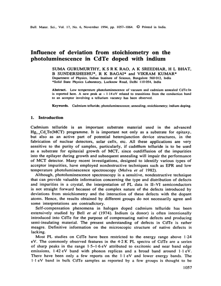
Bull. Mater. Sci., Vol. 17, No. 6, November 1994, pp. 1057-1064. © Printed in India. Influence of deviation from stoichiometry on the photoluminescence in CdTe doped with indium SUMA GURUMURTHY, K S R K RAO, A K SREEDHAR, H L BHAT, B SUNDERSHESHU*, R K BAGAI* and VIKRAM KUMAR* Department of Physics, Indian Institute of Science, Bangalore 560012, India *Solid State Physics Laboratory, Lucknow Road, Delhi 110054, India Low temperature photoluminescence of vacuum and cadmium annealed CdTe:ln is reported here. A new peak at ~ 1.14eV related to transitions from the conduction band to an acceptor involving a tellurium vacancy has been observed. Abstract. Keywords. 1. Cadmiumtelluride; photoluminescence;annealing; stoiehiometry;indium doping. Introduction Cadmium telluride is an important substrate material used in the advanced Hg~_xCd~Te(MCT) programme. It is important not only as a substrate for epitaxy, but also as an active part of potential heterojunction device structures, in the fabrication of nuclear detectors, solar cells, etc. All these applications are very sensitive to the purity of samples, particularly, if cadnl"ium telluride is to be used as a substrate for epitaxial growth of MCT, since outdiffusion of the impurities into the epilayer during growth and subsequent annealing will impair the performance of MCT detector. Many recent investigations, designed to identify various types of acceptor impurities, have employed nondestructive techniques such as EPR and low temperature photoluminescence spectroscopy (Molva et al 1982). Although, photoluminescence spectroscopy is a sensitive, nondestructive technique that can provide valuable information concerning the type and distribution of defects and impurities in a crystal, the interpretation of PL data in I I - V I semiconductors is not straight forward because of the complex nature of the defects introduced by deviations from stoichiometry and the interaction of these defects with the dopant atoms. Hence, the results obtained by different groups do not necessarily agree and some interpretations are contradictory. Self-compensation phenomena in halogen doped cadmium telluride has been extensively studied by Bell et al (1974). Indium (a donor) is often intentionally introduced into CdTe for the purpose of compensating native defects and producing semi-insulating material. The present understanding of defects in CdTe is rather meagre. Definitive information on the microscopic structure of native defects is lacking. Most PL studies on CdTe have been restricted to the energy range above 1-24 eV. The commonly observed features in the 4.2 K PL spectra of CdTe are a series of sharp peaks in the range 1.5-1.6 eV attributed to excitonic and near band edge emissions, 1.42 eV band with phonon replicas and a broad band around 1.1 eV. There have been only a few reports on the 1.1 eV and lower energy bands. The 1-1 eV band in bulk CdTe samples as reported by a few groups is thought to be 1057 1058 Suma GurumurtlL~' et al due to transitions from a deep level formed (de Nobel 1959; Lorentz and Segall 1963; Vavilov et al 1967; Das et al 1990) as a result of deviation from stoichiometry. But, regarding the 1.42 eV defect peak there has been a lot of controversy, with different groups assigning different transitions to it (Vavilov et a! 1967; Rud et al 1971; Das et al 1990; Babentsov et al 1992). Despite the prominence of 1-42 eV bands and their long history of observation, the possible origin of this band still remains a matter of dispute and conjecture. Heat treatments under tellurium or cadmium overpressure are of particular interest because the overall stoichiometry of the crystal can be changed. Suitable conditions for the observation of PL spectra can be achieved, for example, by brief thermal annealing in vapours of the components of the semiconductor. In this paper we report the 4.2 K PL of vacuum and cadmium annealed CdTe doped with indium and the presence of a new peak related to a tellurium vacancy. 2. Experimental Indium doped CdTe crystals, grown by the asymmetrical Bridgman method (Bagai and Borle 1989) have been used in the present investigation. In this method, the growth ampoule is held asymmetrically inside a cylindrical furnace and crystals are grown by lowering the ampoule vertically through the temperature gradient of about 10°C cm -~ at a speed of 0.5 mm h -~. Single crystal wafers of CdTe:In oriented along <111> directions were cut from the grown ingot from which samples of required dimensions were prepared. Typical sample size was 3 x 5 mm ~-. All the cut samples were chemically etched in 1% bromine in methanol for 5 min followed by rinsing for 1 h in methanol to remove traces of bromine. After this, the samples were treated in I N KOH in methanol for 5 min to remove the tellurium film resulting in the bromine methanol etch (Amirtharaj and Pollak 1984). Cadmium annealing was done by placing the CdTe sample in a sealed evacuated dumb bell shaped ampoule in presence of an excess cadmium vapour pressure. The cadmium vapour atmosphere was created by placing a suitable amount of high purity (6 N) cadmium in the ampoule at the same temperature as the CdTe sample. Vacuum annealing was done by placing CdTe sample in a sealed evacuated quartz ampoule without cadmium. Both the annealings were carried out at 650°C for 6 h. Samples were quenched immediately after annealing in liquid nitrogen. A piece of the original sample which was taken from the adjacent part of the wafer and which was not annealed was kept as a control sample (for the sake of comparison). Photoluminescence measurements were carried out at 4.2 K using MIDAC Fourier Transform PL system. An Argon ion laser operating at a wavelength of 5145.~ was used as a source of excitation. The exposed sample area was *- 3 mm 2. Neutral density filters were used to record the spectra at high laser powers. PL signal was detected by a LN 2 cooled Ge-photodetector whose operating range is about 0.75-1.9 eV. Measurements were carried out with a resolution of 0.5 meV. 3. Results and discussion PL measurements were performed on all the pieces cut from a single CdTe:In wafer, prior to annealing treatments. PL spectra recorded were essentially the same Low temperature photoluminescence of CdTe:ln 1059 both in terms of energy position and intensity of the spectral lines. Therefore, any changes which occur in the PL spectra after annealing treatments could be attributed to the changes caused by annealing and not to differences in the starting materials. A typical photoluminescence spectrum of CdTe:In is shown in figure 1. The main features as can be seen are the 1.1 eV broad band (attributed to cadmium vacancies), 1.4 eV peak with phonon replicas (controversial band) and the 1.54 eV edge emission. Figure 2 shows the PL spectra of the 1.11 eV broad band of the control, vacuum and cadmium annealed samples recorded at 4-2 K at a laser excitation power of 100 mW. It is clearly evident from spectra (a) and (b) in this figure that there is a 15 fold increase in the peak height and approximately 8 times increase in the integrated intensity on vacuum annealing. Table I gives the integrated intensity for Ill e4~ ¢.J 13. , 0.9 1.1 1.3 Energy (eV) ~A~, 1.5 Figure 1. PL spectrum of CdTe:ln at 4-2 K in the range 0.9-1.6 eV. (c) ~ x 8 .-I o. (o) ~ 1.0 x 1 5 1.1 1.2 Energy (eV) 1.3 Figure 2. PL spectra at 4.2K showing the I~11 eV band in (a) control. (b) vacuum annealed and (e) cadmium annealed CdTe:ln samples (Excitation power: 100 roW). 1060 Suma Gurumurthy et al various peaks in the control and annealed samples. However, this peak as seen from spectrum (c) is found to have disappeared in the sample annealed in a cadmium atmosphere. This suggests that the band is related to transitions from a native defect involving a cadmium vacancy. Vavilov et al (1967) attributed this band to electron transitions from the doubly charged state of the double acceptor at ( E ¢ - 0 . 6 eV) to the valence band. Sobiesierski e t , a l (1988) have shown that the PL bands at around 1.11 eV in chemically etched bulk samples are a result of deviation from stoichiometry. However, the few reports by Kernocker et al (1985) and Bowman and Cooper (1988) suggest the band around 1.ll eV to arise from some iron impurity. Figure 3 shows the PL spectra of 1.4eV band of the control, vacuum and cadmium annealed samples recorded at 4.2 K at 100 mW laser power. This band which occurs independent of growth technique has not been identified and its origin is therefore widely discussed. This band has the zero phonon line at 1.453 eV. The peak intensity of this band in vacuum annealed sample decreased by approximately 5 times and about 1.5 times in cadmium annealed sample. However, the integrated intensity of this 1.4 eV band in the vacuum annealed sample as can be seen from table 1, decreased by - 1 . 3 times and increased by ~ 1.5 times in the cadmium sample when compared to the control sample. A shift of the peak energy of ~ 4 meV for a decade change in the excitation intensity can be seen from figures 4a Table 1. Integrated intensity of the PL peaks of the control and annealed samples. Laser power (mW) Sample Control Vacuum annealed Cadmium annealed Integrated intensity (au) 1.116 eV I. 146 eV !.4 eV 100 !00 5 39 - 21 16 I00 - 9 35 (c) J ~,~ x 1.5 e6 .-I (3. 1.2 1.3 1./4 1.5 1.6 Energy (eV) I-;gure 3. PL spectra at 4.2 K showing the 1.4 cV band in (a) control, (b) vacuum annealed and (c) cadmium annealed samples. (Excitation power: 100mW). Low temperature photoluminescence o f CdTe:ln I.$ I./) I.II rtmwm, t,v) 1.il 1.1 t,l l.t) ~ 1061 I./)iI 1.1 1.11 (or) l,'igure 4. PL spectra at 4.2 K recorded at different excitation intensities of (a) control and (b) vacuum annealed samples, (Excitation intensities: (a) I0 mW, (b) 50 roW, (c) 150mW and (d) 250 mW). and b for the control and vacuum annealed samples respectively. This shift suggests this band to involve a D--A transition, which is in agreement with earlier reports (Rud et al; 1971, Das et al 1990; Babentsov et al 1992). The transition responsible for this band in all CdTe crystals has been interpreted in various ways. According to de Nobel 0959) the band has been attributed to C-A like transitions. D - A transition has been one of the other interpretation by various groups (Rud et al 19?l; Das et al 1990; Babentsov et al 1992). There has been a lot of speculation regarding the donors and accepters involved in the transition. Some groups have assigned this band to transition from shallow donors to deep accepters involving a cadmium vacancy (Vavilov et al 1967), while others to transition from donors formed by interstitial cadmium atoms to accepters (Vavilov et al 1967; Rud et al 1971). Our results on the effect of cadmium vapour pressure on the luminescence intensity make it difficult to attribute the 1.4 eV band to cadmium vacancy. D-A complex of the type Cd~X may possibly be involved in this transition. However, further investigations must be carried out before any conclusion can be drawn. Investigations by Hofmann et al (1992) clearly show that the emission in this spectral range consists of (at least) thre~ independent emission bands, the first one located at 1.45 eV involving a D-A transition (Chamonal et al 1982), the second one of unknown origin at 1.475 eV (Onodera and Taguchi 1990) and the third one at 1.478 eV (Hofmann et al 1992) arising from a D-A recombination involving the A-centres. It should be noted that all these bands have completely different origins and unfortunately interfere in most of the samples leading to considerable discrepancy. The edge emission at 1-544 eV as seen from figures 3 (spectrum a) and 4a is attributed to a C-A transition as the peak energy does not vary with excitation intensity (Agrinskaya et al 19?l; Barnes, and Zanio 1975). The accepter involved is a singly ionized cadmium vacancy. The hump seen at 1.523 eV is the LO phonon replica of the 1.544 eV peak. Excitation intensity dependence of the peak energy can be seen in figure 4a. However, the edge emission at 1.528 eV as seen from figures 3 (spectrum b) and 4b is a D-A transition as the peak energy shifted by - 4 meV per decade 1062 Suma Gurumurthy et al change in the excitation intensity (Agrinskaya et al 1971). The acceptor is. a cadmium vacancy with an ionization energy of 60 meV as reported earlier. It can be seen from spectrum (c) in figure 3 that the edge emissions have disappeared in the cadmium annealed sample. Spectrum (c) in figure 2 shows a peak at ~ 1.146eV. A level at E , + 0 . 4 6 e V corresponding to a tellurium vacancy has been reported in the literature (Caillot 1972). Halsted et al (1961) for CdTe and Uchida (1964) for ZnS and CdS have shown that a cation deficiency results from firing in an over-pressure of the anion and vice versa. This shows that firing the sample in an over-pressure of cadmium has resulted in the formation of tellurium vacancies and hence the 1.146 eV peak can be attributed to C - A like transitions involving the tellurium vacancy. To confirm the origin of this peak in our spectrum, the cadmium annealed sample was again subjected to a further annealing at 650"C for 6h, but in a saturated tellurium atmosphere. Figure 5 shows the PL spectra of the control, cadmium annealed and subsequent tellurium annealed samples. The disappearance of the 1.146eV peak and reappearance of the 1.116eV peak after tellurium annealing confirms that the 1.146 eV peak is to be related to transitions involving tellurium vacancy. No shift of this peak with excitation intensity was observed. The decrease in the peak intensity of the 1.4 eV band in the tellurium annealed sample as compared to the cadmium annealed one (figure 6), suggests that the 1.4 eV band does not involve a cadmium vacancy. So, firing of the sample in a tellurium atmosphere has resulted in the formation of cadmium vacancies, which is confirmed by the reappearance of the 1-116eV band and the decrease in the intensity of the l-4eV band. The edge emission at 1.532eV as seen from figure 6 (spectrum b) is again a D - A like transition with ~ 10meV/decade shift in the peak energy. A large shift of this magnitude and more has been seen in compensated GaAs (Yu 1977; Swaminathan et al 1981a) and AIGaAs (Mazzaschi et al 1980; Swaminathan et al 1981b) and in moderately dopc~l lnP (Swaminathan et al 1985). Such a large shift with excitation can happen cithc~ when the material is closely compensated or if (c)~ 2 . 2 5 .m t- (b) a. .-# ¢a)~ • . I 1.0 . x2 • . i I I ' ' ' | 1.1 1.2 Energy (eV) ° ' ' ' 1.3 Figure 5. PL spectra at 4.2K showing the I.II6eV and 1.146eV bands in (a) control, (b) cadmium annealed and (e) tellurium annealed subsequent to cadmium annealing samples. (Excitation power: 100 roW). Low temoerature ohotohtminescence of CdTe:ln m r. 1063 x3. c , 1.32 1.40 1.48 Energy (eV) ,_ . ~ o _ 156 ,,igure 6. PL spectra at 4.2K showing the i.4eV band and the edge emissions in (a) cadmium annealed and (b) tellurium annealed subsequent to cadmium annealing samples. (Excitation power: 100 roW). the donor or the acceptor involved is a deep one. More experiments are needed to verify this and work in this direction is under progress. 4. Conclusions Our PL results show the 1.116 eV peak in the vacuum annealed sample to involve cadmium vacancy. The annealing experiments in cadmium and tellurium overpressure suggests that the 1.146 eV peak in cadmium annealed sample to involve a tellurium vacancy and 1.4 eV peak to involve transitions from shallow interstitial cadmium donors to acceptors. Acknowledgement We thank Dr Suman B lyer for helpful discussions. References Agrinskaya N V, Arknd'eva E N and Matveev O A 1971 Soviet Phys. Semicond. 5 762 Amirtharaj P M and Pollak F H 1984 Appl. Phys. Lett. 45 789 Bahentsov V N, Rashkovetskii L V, Sal'kov E A and Tarbaev N 1 1992 Soy. Phys. Semicond. 26 608 and references therein Bagai R K and Bode W N 1989 J. Cryst. Growth 94 561 Barnes C E and Zanio K 1975 J. Appl. Phys. 46 3959 Bell R O, Wald F V, Canali C, Nava F and Ottaviani G 1974 IEEE Trans. Nucl. Sci. NS-21 331 Bowman Jr R C and Cooper D E 1988 Appl. Phys. Lett. 53 1521 Calllot M 1972 Phys. Left. A35 2 Chamonal J P, Molva E and Pautrat J L 1982 Solid State Commun. 43 801 Das S R, Cook J G, Rowell N L and Aoundi M S 1990 J. Appl. Phys. 68 5796 and references therein Halsted R E, Lorenz M R and Segall B 1961 J. Phys. Chem. Solids 22 109 1064 S u m a G u r u m u r t h y et al Hofmann D M, Omling P, Grimmeiss H G, Meyer B IC Benz K W and Sinerius D 1992 Phys. Rev. B45 6247 Kemockef R, Lischka K and Palmetshofer L 1988 J. Cryst. Growth U 625 Lo~ntz M R and Segall B 1963 Phys. Leu. 7 18 M ~ - 7 ~ h i J, Barrau J, Brabant J C, Bmusseau M, Maaref H, VoiUot F and Boissy M C 1980 Rev. Phys. Appl. 15 861 Molva E, Chamonal J P and Pattrat J L 1982 Phys. Status Solidi 11109 635 de Nobel 1959 Philips Res. Rep. 14 361 Onodera C and Taguchi T 1990 J. Cryst. Growth 1el 502 Rud Yu V, Sanin K V and Shreter Yu G 1971 SOy. Phys. SemiconcL $ 573 Sobiesierski Z, Dharmdasa ! M and Williams R H 1988 Appl. Phys. Lett. 53 2623 Swaminathan V, Schumaker N E and Zilko J L 1981a J. Lungn. 22 153 Swaminathan V, Anthony P J, Zilko J L, Sturge M D and Schumaker N E 1981b J. Appl. Phys. ~2 56O3 Swaminathan V, Donnelly V M and Long J 1985 J. Appl. Phys. 58 4565 Uchida I 1964 J. Phys. Soc. J(m 19 670 Vavilov V S, Gippius A A and Panossian J R 1967 Proc. int. ~ II-V! semiconducting coml~Junds (ed.) D G Thomas (New York" Benjamin Inc.) p. 743 Yu P W 1977 J. Appl. Phys. 48 5043
