2.996/6.971 – Lab 3: PCB Layout –
advertisement
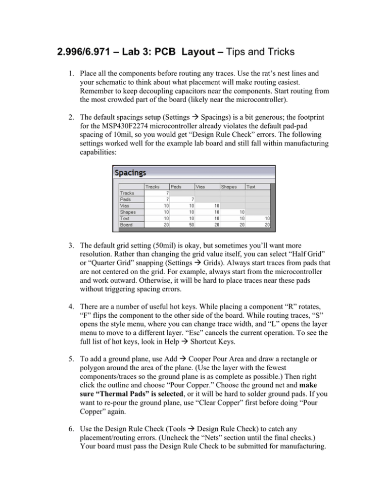
2.996/6.971 – Lab 3: PCB Layout – Tips and Tricks 1. Place all the components before routing any traces. Use the rat’s nest lines and your schematic to think about what placement will make routing easiest. Remember to keep decoupling capacitors near the components. Start routing from the most crowded part of the board (likely near the microcontroller). 2. The default spacings setup (Settings Æ Spacings) is a bit generous; the footprint for the MSP430F2274 microcontroller already violates the default pad-pad spacing of 10mil, so you would get “Design Rule Check” errors. The following settings worked well for the example lab board and still fall within manufacturing capabilities: 3. The default grid setting (50mil) is okay, but sometimes you’ll want more resolution. Rather than changing the grid value itself, you can select “Half Grid” or “Quarter Grid” snapping (Settings Æ Grids). Always start traces from pads that are not centered on the grid. For example, always start from the microcontroller and work outward. Otherwise, it will be hard to place traces near these pads without triggering spacing errors. 4. There are a number of useful hot keys. While placing a component “R” rotates, “F” flips the component to the other side of the board. While routing traces, “S” opens the style menu, where you can change trace width, and “L” opens the layer menu to move to a different layer. “Esc” cancels the current operation. To see the full list of hot keys, look in Help Æ Shortcut Keys. 5. To add a ground plane, use Add Æ Cooper Pour Area and draw a rectangle or polygon around the area of the plane. (Use the layer with the fewest components/traces so the ground plane is as complete as possible.) Then right click the outline and choose “Pour Copper.” Choose the ground net and make sure “Thermal Pads” is selected, or it will be hard to solder ground pads. If you want to re-pour the ground plane, use “Clear Copper” first before doing “Pour Copper” again. 6. Use the Design Rule Check (Tools Æ Design Rule Check) to catch any placement/routing errors. (Uncheck the “Nets” section until the final checks.) Your board must pass the Design Rule Check to be submitted for manufacturing.
