Document 13578743
advertisement
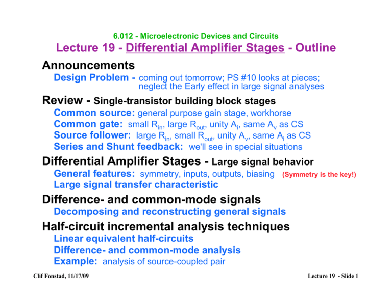
6.012 - Microelectronic Devices and Circuits Lecture 19 - Differential Amplifier Stages - Outline Announcements Design Problem - coming out tomorrow; PS #10 looks at pieces; neglect the Early effect in large signal analyses Review - Single-transistor building block stages Common source: general purpose gain stage, workhorse Common gate: small Rin, large Rout, unity Ai, same Av as CS Source follower: large Rin, small Rout, unity Av, same Ai as CS Series and Shunt feedback: we'll see in special situations Differential Amplifier Stages - Large signal behavior General features: symmetry, inputs, outputs, biasing Large signal transfer characteristic (Symmetry is the key!) Difference- and common-mode signals Decomposing and reconstructing general signals Half-circuit incremental analysis techniques Linear equivalent half-circuits Difference- and common-mode analysis Example: analysis of source-coupled pair Clif Fonstad, 11/17/09 Lecture 19 - Slide 1 Linear amplifier layouts: The practical ways of putting inputs to, and taking outputs from, transistors to form linear amplifiers +V There are 12 choices: three possible nodes to connect to the input, and for each one, two nodes from which to take an output, and two choices of what to do with the remaining node (ground it or connect it to something). Not all these choices work well, however. In fact only three do: Name Common source/emitter +V 2 2 1 1 3 3 IBIAS IBIAS -V -V Input Output Grounded 1 2 3 Common gate/base 3 2 1 Common drain/collector (Source/emitter follower) 1 3 2 1 2 none Source/emitter degeneration Clif Fonstad, 11/17/09 Lecture 19 - Slide 2 • Three MOSFET single-transistor amplifiers V+ V++ ++ vvin in -- CO CO ++ vvout out -IIBIAS BIAS CE + BIAS IIBIAS vout out CII + + v vIN IN -- V -V V -COMMON SOURCE Input: gate Output: drain Common: source Substrate: to source COMMON GATE Input: source; Output: drain Common: gate Substrate: to ground vout + vin - - + + vin - V+ Clif Fonstad, 11/17/09 + + vin IBIAS V- SOURCE FOLLOWER Input: gate Output: source Common: drain Substrate: to source + vin + vout vout - CO + vout - - Lecture 19 - Slide 3 • Single-transistor amplifiers with feedback V+ CO + vout - + vin - RF IBIAS RF + vin - CE CE V- PARALLEL FEEDBACK* SERIES FEEDBACK RF + vin Clif Fonstad, 11/17/09 CO + vout - IBIAS V- + V+ + vout RF - + vin - * Also termed "source degeneracy" vout Lecture 19 - Slide 4 • Summary of the single transistor stages (MOSFET) Voltage gain, Av MOSFET Common source " gm = "gm rl' ) ( [go + gl ] * [ gm + gmb ] rl' Common gate [gm ] *1 g + g + g + g [ m mb o l ] Source degeneracy r *" l (series feedback) RF [ g " GF ] * "g R Shunt feedback " m m F [ go + G F ] Source follower Current gain, Ai Input resistance, Ri # # *1 * 1 [gm + gmb ] Output resistance, Ro $ 1' ro & = ) % go ( + [ gm + gmb + go ] . * ro ,1+ / g 0 t 1 1 * [ gm + go + gl ] gm # # # # * ro g " l GF 1 GF [1" Av ] $ ' 1 ro || RF & = ) g + G [ ] % o F ( Power gain, A p = Av " Ai Clif Fonstad, 11/17/09 Note: When vbs = 0 the gmb factors should be deleted. ! Lecture 19 - Slide 5 • Summary of the single transistor stages (bipolar) Voltage gain, Av BIPOLAR gm = "gm rl' ) ( [ go + gl ] gm Common base = gm rl' ) ( [ go + gl ] [gm + g$ ] Emitter follower +1 g + g + g + g [ m $ o l] r Emitter degeneracy +" l RF [g " GF ] + "g R Shunt feedback " m m F [go + GF ] Common emitter " Current gain, Ai # gl " [go + gl ] +1 Input resistance, R i r$ + r$ [# + 1] Output resistance, R o % 1( ro '= * & go ) + [# + 1] ro # gl +# g + g [ o l] r$ + [# + 1] rl' rt + r$ [# + 1] +# + r$ + [# + 1] RF + ro g " l GF 1 % 1 ( ro || RF ' = * g + G & o F) g$ + GF [1" Av ] Power gain, A p = Av " Ai Clif Fonstad, 11/17/09 Lecture 19 - Slide 6 ! Differential Amplifiers: emitter- and source-coupled pairs V+ + + vIN1 - V+ + vOUT1 vOUT2 - + + vIN2 - + vIN1 - + vOUT1 vOUT2 - IBIAS IBIAS VEmitter-coupled pair + vIN2 - VSource-coupled pair Why do we care? - They amplify only difference-mode signals They are easy to interconnect and cascade They help us eliminate coupling capacitors They are optimally suited to integration Clif Fonstad, 11/17/09 Lecture 19 - Slide 7 Differential Amplifiers: large signal analysis of source coupled pairs Source-coupled pair Below: Schematic with resistor loads Right: Large signal equiv. circuit in saturation +V DD RD M1 + vI1 - RD + vO + + vO1 vO2 - M2 + vI2 - IBIAS Analysis: -V SS 3 KVL loops: vI1 - vGS1 +vGS2 - vI2 = 0, vO1 = VDD - RDiD1, vO2 = VDD - RDiD2 KCL at one node: iD1 + iD2 = IBIAS MOSFET relationships: iD1 = K(vGS1-VT)2/2; iD2 = K(vGS2-VT)2/2 Clif Fonstad, 11/17/09 (see text for details of analysis) Lecture 19 - Slide 8 Diff. Amps: large signal analysis of source coupled pairs, cont. Results: The outputs again only depend on the difference between the two inputs, (vI1 - vI2): # K [v " v ] 2 + I IN1 IN 2 BIAS R % vO1 = VDD " D $ K 4IBIAS 2 2 % + [v IN1 " v IN 2 ] " [v IN1 " v IN 2 ] & 2 K # K [v " v ] 2 + I IN1 IN 2 BIAS RD % vO 2 = VDD " $ K 4IBIAS 2 2 % " [v IN1 " v IN 2 ] " [v IN1 " v IN 2 ] & 2 K vO = " RD K 4I 2 [v IN1 " v IN 2 ] BIAS " [v IN1 " v IN 2 ] 2 K vo ! Symmetrical Slope around origin = -gmRD Clif Fonstad, 11/17/09 Only the difference in the inputs matters!! Lecture 19 - Slide 9 ' % ( % ) ' % ( % ) Differential Amplifiers: large signal analysis of emitter coupled pairs Emitter-coupled pair Below: Schematic with resistor loads Right: Large signal equivalent circuit in FAR +V CC RC Q1 + vI1 - RC + vO + + vO1 vO2 - Q2 + vI2 - IBIAS Analysis: -V EE 3 KVL loops: vI1 - vBE1 +vBE2 - vI2 = 0, vO1 = VCC - RCαFiF1, vO2 = VCC - RCαFiF2 KCL at one node: iF1 + iF2 = IBIAS Ideal diode relationships: iF1 ≈ IES exp (qvBE1/kT), iF2 ≈ IES exp (qvBE2/kT) Clif Fonstad, 11/17/09 (see text for details of analysis) Lecture 19 - Slide 10 Diff. Amps: large signal analysis of emitter coupled pairs, cont. Results: The outputs only depend on the difference between the inputs, (vI1 - vI2): vO1 = VCC " vO 2 = VCC " # F RC IBIAS 1+ e"q ( v I 1 "v I 2 ) kT [ # F RC IBIAS 1+ e q ( v I 1 "v I 2 ) kT [ ] ] q(v I1 " v I 2 ) vO = "# F RC IBIAS tanh 2kT ! Symmetrical Slope around origin = -gmRC Clif Fonstad, 11/17/09 Only the difference in the inputs matters!! Lecture 19 - Slide 11 Differential Amplifier Analysis - difference-mode and common-mode signals Any pair of signals can be decomposed into a portion that is the identical in both, and a portion that is equal, but opposite in both. For example, if we have two voltages, v1 and v2, we can define a common-mode signal, vC, and a difference-mode signal, vD, as: vC = (v1 + v2)/2 vD = v1 - v2 In terms of these two voltages, we can write v1 and v2 as: v1 = vC + vD/2 v2 = vC - vD/2 _______________________________________ In incremental analysis of linear amplifiers we will decompose our inputs into difference- and common-mode inputs: vic = (vin1 + vin2)/2 and vid = vin1 - vin2. We will apply vid to the circuit and get vod (= Avdvid), and then apply vic to the circuit to get voc (= Avcvic). Then we will reconstruct our outputs: vout1 = voc + vod/2 = Avcvic + Avdvid/2 vout2 = voc - vod/2 = Avcvic - Avdvid/2 Clif Fonstad, 11/17/09 Lecture 19 - Slide 12 Differential Amplifier Analysis incremental analysis exploiting symmetry and superposition + vin1 - Linear equivalent circuit (symmetrical) + vout1 - + vin1 - Clif Fonstad, 11/17/09 + vin2 - + vout2 - a LEHC: one half of sym. LEC a LEHC: one half of sym. LEC + vout1 - + vout2 - + vin2 - Lecture 19 - Slide 13 Differential Amplifier Analysis incremental analysis exploiting symmetry and superposition + vid - a LEHC: one half of sym. LEC + vod - + vic - No voltage on common links, so incrementally they are grounded. a LEHC: one half of sym. LEC + voc Clif Fonstad, 11/17/09 a LEHC: one half of sym. LEC + vid - + -vod - a LEHC: one half of sym. LEC No current in common links, so incrementally they are open. + -vid - + voc - a LEHC: one half of sym. LEC + vod = A vdvid - + vic - + vic - a LEHC: one half of sym. LEC + voc = A vc vic Lecture 19 - Slide 14 Differential Amplifier Analysis - example of LEC analysis Consider a source-coupled pair: V+ + vi1 - + vo1 vo2 vi2 IBIAS V- We begin by drawing the LEC for this differential amplifier.... Clif Fonstad, 11/17/09 Lecture 19 - Slide 15 Differential Amplifier Analysis - example, cont. The LEC for our amplifier: gsl g + v in1 gsl d + v gs1 - - g d + gmv gs1 go v o1 - gel gel v o2 go s,b v gs2 gmv gs2 v in2 s,b gcs /2 gcs /2 We decompose our inputs into common- and difference-mode inputs: v id " v in1 # v in 2 Also: v od " v out1 # v out 2 v ic " Clif Fonstad, 11/17/09 v in1 + v in 2 2 v oc " v out1 + v out 2 2 Lecture 19 - Slide 16 Differential Amplifier Analysis - example, cont. With vid and -vid inputs: gsl g + v id d + v gs1 - gsl - g d + go v od - gmv gs1 gel gel -v od go v gs2 gmv gs2 s,b s,b gcs /2 gcs /2 This LEC simplifies to: g + v id =v gs s,b Clif Fonstad, 11/17/09 -v id From which: d + go gsl gmv gs gel v od - s,b Note: We want Avd to be very large. v od = "gm v id (go + gsl + gel ) "gm Avd = ( go + gsl + gel ) Lecture 19 - Slide 17 Differential Amplifier Analysis - example, cont. With vic inputs: gsl g + d + v gs1 v ic gsl g d + go v oc - gmv gs1 - gel gel v oc v gs2 go s,b - s,b gcs /2 gcs /2 This LEC simplifies to: g From which: d + v gs v ic - + go gmv gs v oc " gsl gel v od s,b gcs /2 - Clif Fonstad, 11/17/09 v ic gmv gs2 Note: We want Avc to be very small. ! #gcsv ic 2( gsl + gel ) #gcs Avc " 2( gsl + gel ) Lecture 19 - Slide 18 Differential Amplifier Analysis - example, cont. Knowing Avd and Avc, we can construct vo1 and vo2 : v od A v = Avc v ic + vd id 2 2 gcs gm = " v ic " v id 2( gsl + gel ) 2( go + gsl + gel ) v o1 = v oc + v o2 ! v i1 + v i2 ) gcs gm ( = " " (v i1 " v i2 ) 2( gsl + gel ) 2 2( go + gsl + gel ) v A v = v oc " od = Avc v ic " vd id 2 2 gcs gm = " v ic + v id 2( gsl + gel ) 2( go + gsl + gel ) v i1 + v i2 ) gcs gm ( = " + (v i1 " v i2 ) 2( gsl + gel ) 2 2( go + gsl + gel ) Remember: In a good Diff Amp |Avd| is very large, and |Avc| is very small. Clif Fonstad, 11/17/09 ! Lecture 19 - Slide 19 Looking at a complicated circuit: Lesson I - Find the biasing circuitry and represent it symbolically Consider the following example: Circuitry providing the V REF s + 1.5 V Q1 Q4 Q5 Q6 Q7 Q12 Q11 A A Q16 I BIAS2 Q2 Q8 + vIN1 - Q3 Q4 B Q20 Q9 + vIN2 B I BIAS1 Q13 Q18 Q17 Q21 B Q10 Q14 Q15 + vOUT - Q19 I BIAS3 - 1.5 V 7 of the 21 transistors are used for biasing the other 14 transistors. If we get the biasing transistors out of the picture for awhile, the circuit looks simpler. (next foil) Clif Fonstad, 11/17/09 Lecture 19 - Slide 20 Looking at a complicated circuit: Lesson II - Identify the individual stages and their active transistors and load elements. Actives Continuing with our earlier example, consider the following: Loads + 1.5 V Q4 Q5 Q6 Q7 Q12 Q11 IBIAS2 Q8 Q20 Q9 + vIN1 - + vIN2 - IBIAS1 Source-coupled pair Q13 Q17 Q18 Q21 Q14 Q15 - 1.5 V Pair of commonsource stages PushPull Output Stage (bipolar) + vOUT - IBIAS3 Complementary emitter follower pair (pnp and npn) Note: We can almost make sense of all of the stages, but we still need to study active loads and output stages to fully understand them. Clif Fonstad, 11/17/09 Lecture 19 - Slide 21 Looking at a complicated circuit: Lesson III - Use half-circuit techinques to convert the differential stages to familiar single transistor stages. Continuing with the same example: + 1.5 V Lee Load Q4, Q5, Q6, Q7 (active load) Q8 Q12 Q11 IBIAS2 Q20 Q9 + vIN1 - + vIN2 - Current Mirror Q14, Q15 (active load) with level shift Q13 IBIAS1 Source coupled pair Q17 Q18 Q21 + vOUT - IBIAS3 - 1.5 V Pair of common source stages Complementary emitter followers EF pair (Push-Pull or Totem Pole) There are two symmetrical differential gain stages, followed by two complementary output stages (next foil) Clif Fonstad, 11/17/09 Lecture 19 - Slide 22 Looking at a complicated circuit: Lesson III, cont. - Draw the difference and common mode half circuits. roLL dm Difference mode half circuit: roQ 16 Q12 + vid - Common mode half circuit: Q8 Q20 Q17 roCM dm vod - Q12 Q8 vic 2roQ 10 - RLOAD roQ 16 roLL cm + + Q20 Q17 roCM cm + voc RLOAD - Voila!! We have reduced the transistor count from 21 to 4, and we see that our complex amplifier is just a cascade of 4 single-transistor stages. Clif Fonstad, 11/17/09 Lecture 19 - Slide 23 6.012 - Microelectronic Devices and Circuits Lecture 19 - Differential Amplifier Stages - Summary • Differential Amplifier Stages - Large signal behavior General features: two transistors (a source-coupled, or emitter-coupled, pair) highly symmetrical two inputs, two outputs (Note: one input can be zero) biased by single current source Large signal transfer characteristic: only depends on vIN1 - vIN2 • Difference- and common-mode signals Difference-mode: vID = vIN1 - vIN2 Common-mode: vIC = (vIN1 + vIN2)/2 Reconstruction: vIN1 = vID + vIC/2, vIN2 = vID - vIC/2 • Half-circuit incremental analysis techniques Exploiting symmetry and superposition Difference-mode lin. equiv. half-circuit: links are grounded Common-mode lin. equiv. half circuit: links are cut, open circuited Approach: 1. identify common- and difference-mode half circuits Clif Fonstad, 11/17/09 2. calculate common- and difference-mode signals 3. analyze difference-mode half-circuit (each half-circuit is one of our known building-blocks) 4. analyze common-mode half-circuit 5. reconstruct signals Lecture 19 - Slide 24 MIT OpenCourseWare http://ocw.mit.edu 6.012 Microelectronic Devices and Circuits Fall 2009 For information about citing these materials or our Terms of Use, visit: http://ocw.mit.edu/terms.

