Document 13578717
advertisement

6.012 - Electronic Devices and Circuits
Solving the 5 basic equations - 9/17/09 Version
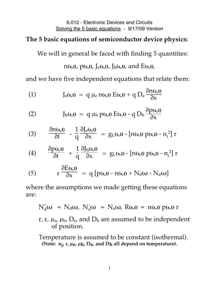
The 5 basic equations of semiconductor device physics:
We will in general be faced with finding 5 quantities:
n(x,t), p(x,t), Je(x,t), Jh(x,t), and E(x,t),
and we have five independent equations that relate them:
(1)
Je(x,t) = q µe n(x,t) E(x,t) + q De
∂n(x,t)
∂x
(2)
Jh(x,t) = q µh p(x,t) E(x,t) - q Dh
∂p(x,t)
∂x
(3)
∂n(x,t)
1 ∂Je(x,t)
2
∂t
q ∂x = gL(x,t) - [n(x,t) p(x,t) - ni ] r
(4)
∂p(x,t)
1 ∂Jh(x,t)
+
=
g
(x,t) - [n(x,t) p(x,t) - ni2] r
L
∂t
q ∂x
(5)
∂E(x,t)
ε ∂x = q [p(x,t) - n(x,t) + Nd(x) - Na(x)]
where the assumptions we made getting these equations
are:
N+d(x) ≈ Nd(x), Na- (x) ≈ Na(x), R(x,t) ≈ n(x,t) p(x,t) r
r, ε, µe, µh, De, and Dh are assumed to be independent
of position.
Temperature is assumed to be constant (isothermal).
(Note: ni, r, µe, µh, De, and Dh all depend on temperature).
1
This is a set of 5 coupled, non-linear differential equations
that are in general not solvable analytically....
BUT we know the solution in three special cases already....
1)
Uniform doping, thermal equilibrium: no, po
(See page 4 below for a discussion of this case)
2)
Drift: g = 0, uniform doping
(See page 4 below for a discussion of this case)
3)
Uniform Low-level Injection: n’, p’, τmin
(See pages 5-6 below for a discussion of this case)
AND we are able to find APPROXIMATE ANALYTICAL
solutions for two very important new situations....
1)
Doping Profile Problems: non-uniformly doped
material in thermal equilibrium (an important
subset of these problems are solved using the
depletion approximation)
(See pages 7-10 below for a discussion of these problems)
2)
Flow Problems: non-uniform injection of excess
carriers into uniformly doped material
(See pages 11-14 below for a discussion of these problems)
********
With an understanding of these solutions to the five
equations we will be able to model and understand all of
the important semiconductor devices, including diodes,
bipolar transistors, and MOSFETs.
(See page 3 for an illustration of this point)
2
Why we care: Understanding Flow Problems, the
Depletion Approximation, and Drift, we can under
stand all of the basic devices we see in 6.012:
Diodes involve flow problems in two regions and the
depletion approximation about one junction:
p-type
n-type
Flow problem
Flow problem
Junctiion problem
Note: This is true not only for simple electronic diodes, but also for light
emitting and laser diodes, and for photodiodes and solar cells.
Bipolar transistors involve flow problems in three regions
and the depletion approximation about two junctions:
B
E
n-type
Junction problem
p
n-type
C
Flow problems
MOSFETs involve two diodes, the depletion approxi
mation in the gate region, and drift in the channel:
G
S
n+
Diodes
D
n+
p-type
Depletion approximation
Drift
3
Special Case: UNIFORM DOPING, THERMAL EQUIL.
Uniform material, thermal equilibrium: ∂/∂x = 0,
∂/∂t ≈ 0, and gL = 0. In this case n and p are constant and
denoted as no and po. Equations 3 and 4 give: nopo = ni2,
and Equation 5 gives: po - no + Nd - Na = 0. Combining
and solving for no and po yields:
when Nd - Na >> ni (i.e., n-type), no ≈ Nd - Na, and po = ni2/no
and
when Na - Nd >> ni (i.e., p-type), po ≈ Na - Nd, and no = ni2/po
Special Case: DRIFT
Uniform material; uniform, slowly varying (quasi
static) externally applied electric field: ∂/∂x = 0, ∂/∂t ≈ 0,
and gL = 0.
Equations (3) and (4) yield: np = ni2, and Equation (5)
yields: p - n + Nd - Na = 0. Combining these we see p and
n are the same as po and no in thermal equilibrium.
Using this with Equations (1) and (2) yields:
Je(t) = q µe no E(t),
Jh(t) = q µh po E(t)
JTOT(t) = Je(t) + Jh(t) = q (µe no + µh po) E(t)
We see that under these conditions we have a current
proportional to any externally applied electric field. This
is Ohm's law on a microscopic scale.
4
Special Case: UNIFORM OPTICAL EXCITATION
(Photoconductivity)
(Minority Carrier Lifetime)
Uniform material; uniform optical generation, gL(t);
uniform applied electric field; low level injection:
∂/∂x = 0
******
We first define excess carrier populations, n' and p', as:
n(t) = no + n'(t),
p(t) = po + p'(t),
or
or
n'(t) = n(t) - no
p'(t) = p(t) - po
Symmetry tells us we must have zero internal electric
field, and since any externally applied electric field must
be uniform, there is no gradient in the electric field. Using
this in Equation (5), yields
n'(t) = p'(t)
Using all of this in Equations (1) and (2) shows us that we
only have drift currents, but they are larger than in
thermal equilibrium. This is photoconductivity:
Je(x,t) = q µe [no + n'(t)] E,
Jh(x,t) = q µh [po + p'(t)] E
JTOT(t) = [q (µe no + µh po) + q (µe + µh) n'(t)] E
"thermal equilibrium conductivity"
"photoconductivity"
Returning now to p'(t) and n'(t), which are still unknowns,
we know they are equal, and to determine what they are
we use either Equation (3) or Equation (4):
5
dn(t)
dt
yielding
=
dn'(t)
=
g
(t) - [{no + n'(t)}{po + p'(t)} - ni2] r
L
dt
dn'(t)
dt = gL(t) - [{no + po +n'(t)} n'(t)}] r
To linearize this first order differential equation we
assume low level injection, i.e. n'(t) << no + po. This sum is
essentially the majority carrier population, and we will
focus on the excess minority carrier population.
Assuming for sake of discussion that we have a p-type
sample, we normally would write this as n'(t) << po. In
this case we have
{no + po +n'(t)} ≈ po
and thus
dn'(t)
dt ≈ gL(t) - n'(t) po r
We define the minority carrier lifetime, τe, as 1/po r, so:
dn'(t)
n'(t)
+
τe ≈ gL(t)
dt
This is a first order, linear differential equation well
known to us from RC circuits. The homogeneous
solutions of this equation are of the form:
n'(t) = A e-t/τ e
where A is chosen so that the total solution (homoge
neous plus particular) satisfies the initial condition.
6
Special Case: DOPING PROFILES and JUNCTIONS
Arbitrary doping profile; thermal equilibrium:
∂/∂t = 0, gL = 0; arbitrary Nd(x), Na(x)
******
In thermal equilibrium the currents must be zero so from
Equations (3) and (4) we find that even with an arbitrary
doping profile,
no(x) po(x) = ni2,
and Equations (1) and (2) tell us that
0 = q µe no(x) E(x) + q De
dno(x)
dx
0 = q µh po(x) E(x) - q Dh
dpo(x)
dx
and
We can rewrite these equations using E(x) = -dΦ(x)/dx
as:
µe dΦ(x)
1 dno(x)
=
no(x) dx
De dx
and
µh dΦ(x)
1 dpo(x)
=
po(x) dx
Dh dx
Integrating both sides with respect to x, and adapting the
convention that Φ(x) is zero in intrinsic material, i.e., where
no(x) = po(x) = ni, we have
no(x) = ni e
7
µe
De
Φ(x)
and
po(x)
µh
= ni e - Dh Φ(x)
We see immediately that the requirement that no(x) po(x) =
ni2, tells us that we must have:
µe
µh
=
De
Dh
In fact, the ratio of µ to D is equal to a very specific
quantity, q/kT:
µe
µh
q
=
=
De
Dh
kT
This equality is known as the Einstein relation; it is easy to
remember because it rhymes as written, and it also
rhymes inverted. We use it frequently.
We thus have:
and
no(x) = ni e qΦ(x)/kT
po(x) = ni e - qΦ(x)/kT
Alternatively, we can write in terms of no(x) and/or po(x):
no(x)
po(x)
kT
kT
Φ(x) = q ln n = - q ln n
i
i
Finally, we use these results in Equation (5) (which also
relates Φ(x), po(x), and no(x)) to write:
∂2Φ(x)
ε ∂x2 = q [ni e - qΦ(x)/kT- ni e qΦ(x)/kT+ Nd(x) - Na(x)]
8
Once again we have reduced our five equations to one
equation in one unknown (Φ(x) in this case). However, the
solution of this equation is, in general, impossible to
obtain analytically, but it can easily be solved iteratively
by computer, and in many cases a perfectly adequate
solution can be found by hand using the "depletion
approximation".
An important observation is that the electrostatic
potential, Φ(x), depends only logarithmically on the
equilibrium carrier concentrations, po(x) and no(x). This
means that large changes in carrier concentration result in
only relatively small changes in the electrostatic potential.
Said the other way around, a small change in electrostatic
potential corresponds to a relatively large change in the
carrier concentrations. A useful rule of thumb to keep in
mind is that an order of magnitude change in carrier
concentration, corresponds to a 60 mV change in
electrostatic potential. This is called "The 60 mV rule."
Special Profiles
Gradual spatial variation: If Nd(x) and/or Na(x) vary only
slowly with position (where "slowly" can be defined using
the concept of Debye length), the equilibrium carrier
concentrations track the doping profile, i.e. in an n-type
sample where, Nd(x) - Na(x) > 0
no(x) ≈ Nd(x) - Na(x) and po(x)
=
ni2/no(x)
Abrupt doping changes; depletion approximation: If the
doping changes abruptly, for example from p-type to ntype at a p-n junction, the majority carrier concentration
will fall so quickly at the electrostatic potential begins to
9
change that a "depletion region", i.e., a region effectively
void of mobile carriers will be created. In that region there
will be a net charge density approximately equal to that of
the net donor or acceptor concentration.
For example, if the depletion region on the n-side extends
from 0 to xn, the depletion approximation says that net
charge density, ρ(x), can be approximated as:
ρ(x) ≈ q[Nd(x) - Na(x)] for 0 < x < xn
The depletion approximation model gives an estimate for
the net charge density profile. Having this estimate, we
can integrate it once to get an estimate for the electric field
profile, E(x). Integrating again gives us an estimate for the
electrostatic potential profile, Φ(x). Having this we can
calculate no(x) and po(x), recalculate ρ(x), etc., and continue
interating until we are satisfied. Usually we stop after one
time through, i.e., after calculating Φ(x) the first time.
10
Special Case: FLOW PROBLEMS
Uniform material; quasi-static (slowly varying), low
level optical excitation of arbitrary distribution, i.e. gL(x,t);
no externally applied electric field (may have internal
field):
∂/∂t ≈ 0; n', p' << no + po
Assume p-type for purposes of discussion.
******
We already know no and po in this situation, so the
problem is one of finding the excess carrier populations,
the currents, and the electric field.
A fundamental assumption we make is that the material
remains essential charge neutral. We call this condition
quasineutrality, and specify it by saying that we can
assume
p'(x,t) ≈ n'(x,t), and ∂n'(x,t)/∂x ≈ ∂p'(x,t)/∂x
We will not justify this assumption rigorously in 6.012, but
one can show that it is well satisfied in semiconductors.
You can refer to Appendix D in the course text for more.
We proceed with Equation (3), which yields:
1 ∂Je(x,t)
n'(x,t)
- q ∂x ≈ gL(x,t) - τe
We next turn to Equations (1) and (2), and we argue that
any minority carrier drift must be negligible under low
level injection conditions. The minority carrier drift
11
current is always much less than the majority carrier drift
current, so the only way there will be a non-negligible
minority carrier current is if it is a minority carrier
diffusion current. Thus, in our present case of a p-type
sample, Equation (1) becomes:
Je(x,t) ≈ q De
∂n'(x,t)
∂x
Combining the last two equations yields a single second
order differential equation in the minority carrier
concentration:
gL(x,t)
n'(x,t)
∂2n'(x,t)
≈
Deτe
De
∂x2
The homogeneous solutions of this equation are of the
form:
n'(x,t) = A e-x/Le + B e+x/Le
where we have defined the minority carrier diffusion
length, Le, as
Le = Deτe
The constants A and B are chosen so that the total
solution, consisting of the sum of the homogeneous
solution and the particular solutiion, satisfy the boundary
conditions.
Now we can continue to calculate the rest of the quantities
of interest, i.e., p'(x,t), Je(x,t), Jh(x,t), and E(x,t). We begin by
noticing that once we know n'(x,t), we can calculate Je(x,t)
using the equation above.
12
Then we calculate Jh(x,t) using JTot(t) = Je(x,t) + Jh(x,t). We will
in general know what JTot(t) is from the problem statement,
or from some other piece of information. To see that JTot(t)
is not a function of position in quasistatic situations (i.e.,
∂/∂t ≈ 0), subtract Equations (3) and (4) to get:
∂Je(x,t)
∂Jh(x,t)
∂[Je(x,t) + Jh(x,t)]
∂JTot(t)
+
=
=
∂x
∂x
∂x
∂x = 0
Knowing Jh(x,t), we calculate E(x) using Equation (2), along
with our assumptions of low level injection (i.e., p(x,t) ≈ po)
and quasineutrality (i.e., ∂n'(x,t)/∂x ≈ ∂p'(x,t)/∂x).
Once we have E(x), we calculate p'(x) using Equation (5).
Finally, we look at all of our answers and confirm that all
of our assumptions were valid. If they are, we are done.
If they are not, we start over, this time not making the
invalid assumptions.
Boundary Conditions
An important aspect of solving flow problems is knowing
the boundary conditions. Once you know the boundary
conditions, you can often sketch the answer (usually the
excess minority carrier distribution). The key boundary
conditions we encounter in 6.012 can be summarized as
follows:
ohmic contacts - excesses are identically zero
reflecting surfaces - net current in or out is zero (i.e.
slope of minority carrier profile is zero) unless there
is surface generation, in which case the flux away
from the surface equals the generation rate
13
internal boundaries - excess concentration profiles are
never discontinuous; the current can only be
discontinuous if there is generation/recombination
in the boundary plane, in which case the net flux
out/in equals the generation/recombination rate
injecting surface/boundaries - in devices we will have
boundaries which establish the value of (a) the
excess minority carrier population, or (b) the excess
minority carrier flux (current density)
Infinite Lifetime Approximation
In cases where the minority carrier diffusion length, Le, is
much larger than the dimensions of the sample, we can
often ignore the n'/ Le2 term in the diffusion equation, so
that our equation becomes simply
gL(x,t)
∂2n'(x,t)
≈
De
∂x2
Important points to make about this result are:
1. We can find n’ for an arbitrary gL simply by
integrating this equation twice, and then using the
boundary conditions to get the two constants of
integration.
2. When gL is zero, the profiles are straight lines.
3. This is called the infinite lifetime approximation
because it is equivalent to neglecting recombination.
14
MIT OpenCourseWare
http://ocw.mit.edu
6.012 Microelectronic Devices and Circuits
Fall 2009
For information about citing these materials or our Terms of Use, visit: http://ocw.mit.edu/terms.


