6.012 MICROELECTRONIC DEVICES AND CIRCUITS
advertisement
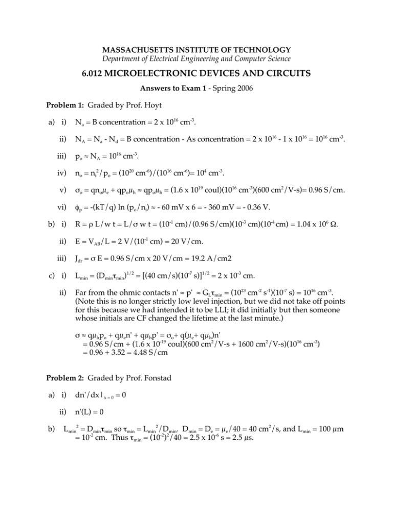
MASSACHUSETTS INSTITUTE OF TECHNOLOGY Department of Electrical Engineering and Computer Science 6.012 MICROELECTRONIC DEVICES AND CIRCUITS Answers to Exam 1 - Spring 2006 Problem 1: Graded by Prof. Hoyt a) i) Na = B concentration = 2 x 1016 cm-3. ii) NA = Na - Nd = B concentration - As concentration = 2 x 10¹⁶ - 1 x 1016 = 1016 cm-3. iii) po ≈ NA = 1016 cm-3. iv) no = ni2/po = (1020 cm-6)/(1016 cm-6)= 104 cm-3. v) σo = qnoµe + qpoµh ≈ qpoµh = (1.6 x 10¹⁹ coul)(1016 cm-3)(600 cm2/V-s)= 0.96 S/cm. vi) φp = -(kT/q) ln (po/ni) ≈ - 60 mV x 6 = - 360 mV = - 0.36 V. b) i) R = ρ L/w t = L/σ w t = (10-1 cm)/(0.96 S/cm)(10-3 cm)(10-4 cm) = 1.04 x 10⁶ Ω. ii) E = VAB/L = 2 V/(10-1 cm) = 20 V/cm. iii) Jdr = σ E = 0.96 S/cm x 20 V/cm = 19.2 A/cm2 c) i) ii) Lmin = (Dminτmin)1/2 = [(40 cm/s)(10-7 s)]1/2 = 2 x 10⁻³ cm. Far from the ohmic contacts n' ≈ p' ≈ GLτmin = (1023 cm-2 s-1)(10-7 s) = 1016 cm-3. (Note this is no longer strictly low level injection, but we did not take off points for this because we had intended it to be LLI; it did initially but then someone whose initials are CF changed the lifetime at the last minute.) σ ≈ qµhpo + qµen' + qµhp' = σo+ q(µe+ qµh)n' = 0.96 S/cm + (1.6 x 10⁻¹⁹ coul)(600 cm2/V-s + 1600 cm2/V-s)(1016 cm-3) = 0.96 + 3.52 = 4.48 S/cm Problem 2: Graded by Prof. Fonstad a) i) ii) b) dn'/dx|x = 0 = 0 n'(L) = 0 Lmin2 = Dminτmin so τmin = Lmin2/Dmin. Dmin = De = µe/40 = 40 cm2/s, and Lmin = 100 µm = 10-2 cm. Thus τmin = (10-2)2/40 = 2.5 x 10⁻⁶ s = 2.5 µs. c) i) D, because the minority carrier diffusion flux must be zero at x = 0, and the flux builds up (increases) linearly because there is uniform optical creation of holeelectron pairs and no appreciable recombination. Alternatively one could say that the integral of the generation function (a constant in this case) yields the gradient in the excess population, and the flux proportional to this. The integral of a constant is a line of constant slope. ii) A, because it is consistent with the answer in (i), because it is the only profile that fits the boundary conditions, and/or it is what one gets by integrating a constant twice. d) With no recombination the total flux density into the ohmic contact must be the the total generation within the sample, which is the integral of gL(x) from x = 0 to x = L. In this case gL(x) is a constant, call it GL, so the integral is GLL. The current density is the charge per carrier, -q, times the flux: Jmin(x) = -q GLL = -1.6 x 10-19 x 1019 x 10-3 = -1.6 x 10⁻³ A/cm2 = -1.6 mA/cm2. e) i) The recombination at any point is n'(x)/τmin, so the total recombination per unit area is ∫0→L[ n'(x)/τmin]dx. If one finds n'(x) and does this integral you get GLL3/3τminDmin = GLL3/3Lmin2. The numerical answer is 3.2 x 1013 cm-2s-1. ii) Much greater than, because even though there is non-zero recombination in the bulk, it is still much less than occurs at the ends. If one compares the answers in Parts (d) and (e-i), one sees that the fraction recombining in the bulk is L2/3Lmin2. In this case this is 1/300, so 300 times as much recombination occurs at the contact as within the bulk. The important concept upon which Part (e) of this problem is based is that one can find the excess carrier and flux profiles in a short base situation (i.e., long diffusion length) assuming that the lifetime in infinite, and then turn around and find out how much recombination occurs (and this how good the initial assumption was) by using the true minority carrier lifetime and the profile calculated assuming infinite lifetime to estimate the amount of recombination. Comparing this to the total minority carrier generation and/or injection, or to the recombination fluxes at the contacts. Problem 3: Graded by Prof. Antoniadis a) i) 0.84 V using the 60 mV rule; 0.81 V if use kT = 0.025 V and evaluate the exponential. ii) 1 µm iii) Je/Jh = (De/Dh)(ND/NA1)[wn/(wp-xp)] = 3 x (1/3) x b) i) Same as (a-i). ii) xp ≈ [2εSi(φb-V1)/qNA1)]1/2 so V1 = -(qNA1xp2/2εSi) + φb = -2.4 V iii) The small signal linear equivalent capacitance is the same as a parallel plate capacitor with the same width as the depletion region and the dielectric constant of silicon: Cab(V1) = eSi/w(V1) ≈ εSi/xp(V1) = 10-12/2 x 10-4 = 5 x 10⁻⁹ F/cm2. iv) Figure b because xp will increase only marginally for vAB > V1 due to NA2 >> NA1. Consequently, the depletion region width, w, which is essentially the same as xp, will not increase either. The capacitance per unit area, Cab, is εSi/w, so it will not decrease appreciably for vAB > V1. Average/Standard deviation: Problem 1 Problem 2 Problem 3 Total 29.4 24.4 23.9 77.8 4.5 5.3 5.3 11.9 Distribution to nearest 5: Find your face in this picture 20 30 40 50 60 Total Score 70 80 90 100 MIT OpenCourseWare http://ocw.mit.edu 6.012 Microelectronic Devices and Circuits Fall 2009 For information about citing these materials or our Terms of Use, visit: http://ocw.mit.edu/terms.
