A Two-Step Incremental Analog-to-Digital Converter
advertisement

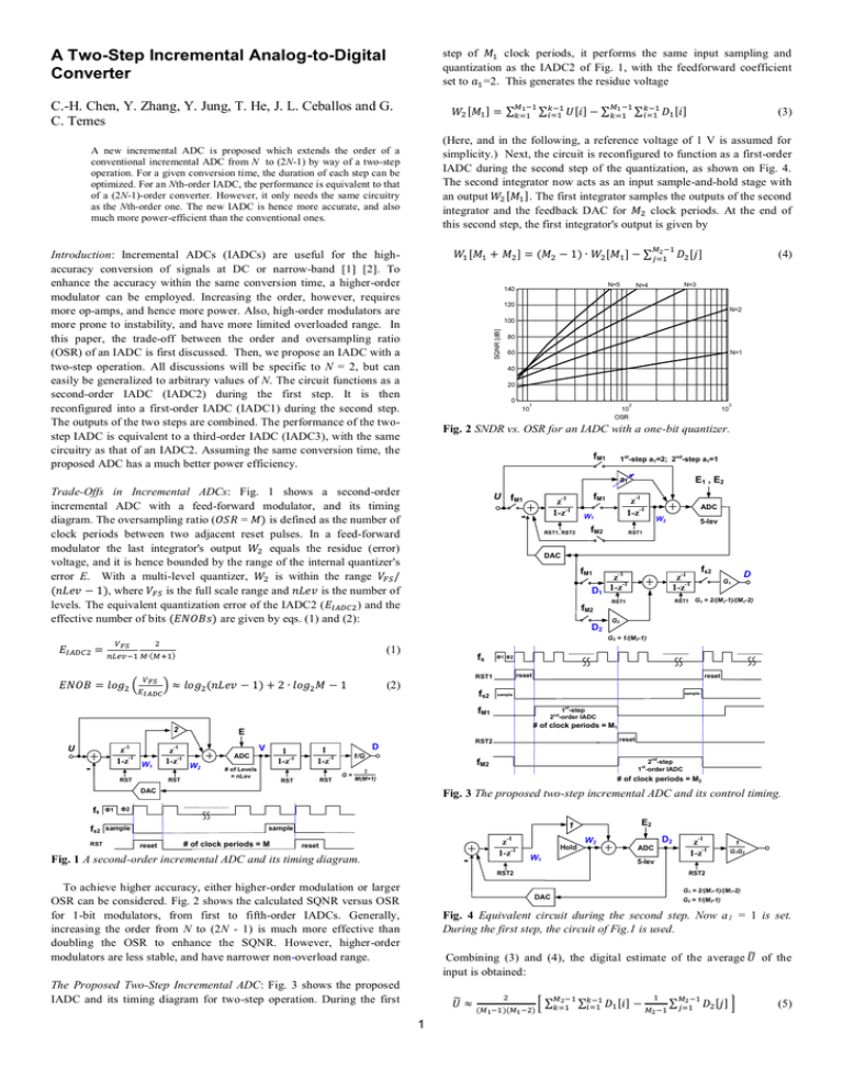
step of clock periods, it performs the same input sampling and quantization as the IADC2 of Fig. 1, with the feedforward coefficient set to =2. This generates the residue voltage A Two-Step Incremental Analog-to-Digital Converter C.-H. Chen, Y. Zhang, Y. Jung, T. He, J. L. Ceballos and G. C. Temes [ ] ∑ ∑ [] ∑ ∑ [] (3) (Here, and in the following, a reference voltage of 1 V is assumed for simplicity.) Next, the circuit is reconfigured to function as a first-order IADC during the second step of the quantization, as shown on Fig. 4. The second integrator now acts as an input sample-and-hold stage with [ ]. The first integrator samples the outputs of the second an output integrator and the feedback DAC for clock periods. At the end of this second step, the first integrator's output is given by A new incremental ADC is proposed which extends the order of a conventional incremental ADC from N to (2N-1) by way of a two-step operation. For a given conversion time, the duration of each step can be optimized. For an Nth-order IADC, the performance is equivalent to that of a (2N-1)-order converter. However, it only needs the same circuitry as the Nth-order one. The new IADC is hence more accurate, and also much more power-efficient than the conventional ones. [ Introduction: Incremental ADCs (IADCs) are useful for the highaccuracy conversion of signals at DC or narrow-band [1] [2]. To enhance the accuracy within the same conversion time, a higher-order modulator can be employed. Increasing the order, however, requires more op-amps, and hence more power. Also, high-order modulators are more prone to instability, and have more limited overloaded range. In this paper, the trade-off between the order and oversampling ratio (OSR) of an IADC is first discussed. Then, we propose an IADC with a two-step operation. All discussions will be specific to N = 2, but can easily be generalized to arbitrary values of N. The circuit functions as a second-order IADC (IADC2) during the first step. It is then reconfigured into a first-order IADC (IADC1) during the second step. The outputs of the two steps are combined. The performance of the twostep IADC is equivalent to a third-order IADC (IADC3), with the same circuitry as that of an IADC2. Assuming the same conversion time, the proposed ADC has a much better power efficiency. ] [ ] ∑ N=5 140 [] (4) N=3 N=4 120 N=2 SQNR [dB] 100 80 60 N=1 40 20 0 10 1 10 OSR 2 10 3 Fig. 2 SNDR vs. OSR for an IADC with a one-bit quantizer. fM1 1st-step a1=2; 2nd-step a1=1 E1 , E2 a1 Trade-Offs in Incremental ADCs: Fig. 1 shows a second-order incremental ADC with a feed-forward modulator, and its timing diagram. The oversampling ratio ( = is defined as the number of clock periods between two adjacent reset pulses. In a feed-forward modulator the last integrator's output equals the residue (error) voltage, and it is hence bounded by the range of the internal quantizer's error E. With a multi-level quantizer, is within the range , where is the full scale range and is the number of levels. The equivalent quantization error of the IADC2 ( ) and the effective number of bits are given by eqs. (1) and (2): U fM1 fM1 -1 z 1-z-1 - -1 z 1-z-1 W1 fM2 RST1, RST2 ADC W2 5-lev RST1 DAC fM1 D1 fM2 D2 z-1 1-z-1 z-1 1-z-1 RST1 RST1 fs2 D G1 G1 = 2/(M1-1)/(M1-2) G2 G2 = 1/(M2-1) (1) ( fs Φ1 Φ2 reset RST1 ) (2) fs2 reset sample sample 1st-step 2nd-order IADC fM1 2 z-1 1-z-1 W 1 U - RST z-1 1-z-1 RST # of clock periods = M1 E V 1 1-z-1 ADC W2 # of Levels = nLev D 1 1-z-1 RST RST 1/G G= fs2 RST Φ1 2nd-step 1st-order IADC fM2 2 M(M+1) # of clock periods = M2 DAC fs reset RST2 Fig. 3 The proposed two-step incremental ADC and its control timing. Φ2 sample reset # of clock periods = M E2 1 sample -1 reset - Fig. 1 A second-order incremental ADC and its timing diagram. z 1-z-1 Hold D2 W2 ADC W1 1 G1G2 5-lev RST2 RST2 To achieve higher accuracy, either higher-order modulation or larger OSR can be considered. Fig. 2 shows the calculated SQNR versus OSR for 1-bit modulators, from first to fifth-order IADCs. Generally, increasing the order from N to (2N - 1) is much more effective than doubling the OSR to enhance the SQNR. However, higher-order modulators are less stable, and have narrower non-overload range. z-1 1-z-1 G1 = 2/(M1-1)/(M1-2) DAC G2 = 1/(M2-1) Fig. 4 Equivalent circuit during the second step. Now a 1 = 1 is set. During the first step, the circuit of Fig.1 is used. Combining (3) and (4), the digital estimate of the average ̃ of the input is obtained: The Proposed Two-Step Incremental ADC: Fig. 3 shows the proposed IADC and its timing diagram for two-step operation. During the first ̃ 1 [∑ ∑ [] ∑ [ ]] (5) The modulator insures W1 < and as a second-order one (plus some simple timing control). It is therefore much more power-efficient for high-accuracy data conversion. and hence the quantization error of the two-step ADC can be estimated from Acknowledgement: This work was supported by Infineon Technologies. (6) C.-H. Chen, Y. Zhang, Y. Jung, T. He and G. C. Temes (School of EECS, Oregon State University, Corvallis, OR, 97330, USA) E-mail: chench@eecs.oregonstate.edu J. L. Ceballos (Infineon Technologies Austria AG, Siemensstrasse 2, 9500 Villach, Austria) E-mail: joseluis.ceballos@infineon.com The re-configuration between the two steps can be easily implemented by multiplexing the two integrators with the timing control shown in Fig. 3. The total OSR is divided into two terms and ( ). Selecting and the ENOB of (6) can be optimized to a value (7) References 1 J. Markus, J. Silva, and G. C. Temes, “Theory and applications of incremental ΔΣ converters,” IEEE Trans. Circuits Syst. I, vol. 51, pp. 678–690, Apr. 2004 For the same conversion time, a comparison of eqs. (2) and (7) shows that the two-step IDC's optimal ENOB is larger by than that of an IADC2. The difference is positive for M > 7. Applying the two-step scheme to an Nth order IADC, during the second step it is reconfigured as a (N-1)th order IADC, and achieves a (2N -1)th-order modulation. For general N, the optimum partition of conversion time is . A two-step IADC scheme was published earlier [3], but it needed an extra op-amp to perform sample-hold operation, and it used a 1st-order algorithmic ADC during the first step. 2 C.-H. Chen, J. Crop, J. Chae, P. Chiang and G. C. Temes, “A 12-bit 7µW/channel 1kHz/channel incremental ADC for biosensor interface circuits,” IEEE Int. Symp. on Circuits and Systems, 2012 3 G. Mulliken, F. Adil, G. Cauwenberghs, and R. Genov, “Delta–sigma algorithmic analog-to-digital conversion,” IEEE Int. Symp. on Circuits and System (ISCAS), 2002. Simulation Results: The proposed two-step IADC was simulated for a 40 Hz signal bandwith, and with M = OSR = 96. A five-level quantizer was used. The optimal selection of and was then = 64 and = 32. The SQNR versus is shown on Fig. 5, confirming this choice. Fig. 6 shows the simulated PSD with a -3dBFS signal amplitude. The SQNR is 103 dB. With the same circuitry and OSR, the IADC2 of Fig. 1 results in 83 dB. The improvement is consistent with the increased ENOB of (7). The conventional third-order IADC gives SQNR = 103 dB. The proposed two-step second-order IADC is thus equivalent to a third-order IADC in performance. However, the required analog circuitry is same as for the IADC2. It only needs some simple additional digital circuits to perform the timing control. 110 SQNR [dB] 105 100 95 90 0 10 20 30 40 50 60 70 80 90 # of clock periods during 1st-step (M1) Fig. 5 SQNR vs. M1 for the two-step IADC. The total OSR is 96. 2-Step Incremental ADC; VP= -3dB; Freq=23Hz; CLK=8.192kHz; Magnitude [dB] 0 IDC2 only 2-step IDC -50 IDC2; SNR = 83.3dB 2-step IDC; SNR = 102.7dB -100 -150 0 5 10 15 20 25 Frequency [Hz] 30 35 40 Fig. 6 Simulated power spectral densities with a -3 dBFS signal. Conclusions: A two-step IADC is proposed to perform residue quantization. It functions as a IADC2 during the first step, and it is reconfigured as a IADC1 during the second step. Its performance is equivalent to that of a third-order IADC, but it needs the same circuitry 2


