Isolated, Linearized, Thermocouple Input
3B47
FEATURES
Interfaces, amplifies, filters, isolates, & linearizes analog
input voltages from a J, K, T, E, R, S or B-type thermocouple
Thermocouple input signal is internally linearized
High accuracy internal cold junction compensation.
Module provides +1500 V peak of galvanic transformerbased isolation with a common mode rejection (CMR) of 160
dB @ 50/60 Hz and a normal mode rejection (NMR) of 60 dB
@ 50/60 Hz.
All 3B47 series modules are mix-and-match and Hot
Swappable.
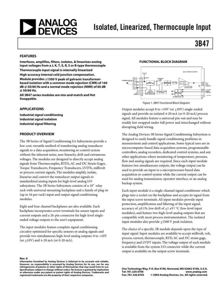
FUNCTIONAL BLOCK DIAGRAM
Figure 1. 3B47 Functional Block Diagram
APPLICATIONS
Industrial signal conditioning
Industrial signal isolation
Industrial signal filtering
PRODUCT OVERVIEW
The 3B Series of Signal Conditioning I/o Subsystems provide a
low-cost, versatile method of transferring analog transducer
signals to a data acquisition, monitoring or control system
without the inherent noise, non-linearity, drift and extraneous
voltages. The modules are designed to directly accept analog
signals from Thermocouples, RTD’s, AC and DC Strain Gages,
Torque Transducers, Frequency Transducers, LVDTs, millivolt
or process current signals. The modules amplify, isolate,
linearize and convert the transducer output signals to
standardized analog inputs for high-level analog I/O
subsystems. The 3B Series Subsystem consists of a 10” relay
rack with universal mounting backplane and a family of plug-in
(up to 16 per rack) input and output signal conditioning
modules.
Eight and four channel backplanes are also available. Each
backplane incorporates screw terminals for sensor inputs and
current outputs and a 26-pin connector for high-level singleended voltage outputs to the user’s equipment.
The input modules feature complete signal conditioning
circuitry optimized for specific sensors or analog signals and
provide two simultaneous high-level analog outputs: 0 to +10V
(or +10V) and 4-20 mA (or 0-20 mA).
Output modules accept 0 to +10V (or +10V) single-ended
signals and provide an isolated 4-20 mA (or 0-20 mA) process
signal. All modules feature a universal pin-out and may be
readily hot-swapped under full power and interchanged without
disrupting field wiring.
The Analog Devices 3B Series Signal Conditioning Subsystem is
designed to easily handle signal conditioning problems in
measurement and control applications. Some typical uses are in
microcomputer-based data acquisition systems, programmable
controllers, analog recorders, dedicated control systems, and any
other applications where monitoring of temperature, pressure,
flow and analog signals are required. Since each input module
features two simultaneous outputs, the voltage output can be
used to provide an input to a microprocessor-based data
acquisition or control system while the current output can be
used for analog transmission, operator interface, or an analog
backup system.
Each input module is a single-channel signal conditioner which
plugs into a socket on the backplane and accepts its signal from
the input screw terminals. All input modules provide input
protection, amplification and filtering of the input signal,
accuracy of +0.1%, low drift of +1 uV/ oC (low-level input
modules), and feature two high-level analog outputs that are
compatible with most process instrumentation. The isolated
input modules also provide +1500 V peak isolation.
The choice of a specific 3B module depends upon the type of
input signal. Input modules are available to accept millivolt, volt,
process current, thermocouple, RTD, AC and DC strain gage,
frequency and LVDT inputs. The voltage output of each module
is available from the system I/O connector while the current
output is available on the output screw terminals.
Rev. 0
Information furnished by Analog Devices is believed to be accurate and reliable.
However, no responsibility is assumed by Analog Devices for its use, nor for any
infringements of patents or other rights of third parties that may result from its use.
Specifications subject to change without notice. No license is granted by implication
or otherwise under any patent or patent rights of Analog Devices. Trademarks and
registered trademarks are the property of their respective companies.
One Technology Way, P.O. Box 9106, Norwood, MA 02062-9106, U.S.A.
www.analog.com
Tel: 781.329.4700
Fax: 781.326.8703
© 2004 Analog Devices, Inc. All rights reserved.
3B47
GENERAL DESCRIPTION
CUSTOM). Zero suppression can exceed 100% of the input
range. This enables suppression of a zero-scale input value
many times larger than the total span for precise expandedscale measurements of a selection portion of an input signal.
The differential input circuit on the field side is fully floating,
eliminating the need for any input grounding. Signal isolation
by transformer coupling uses a proprietary modulation
technique for linear, stable and reliable performance. A
demodulator on the computer side of the signal transformer
recovers the original signal which is then filtered and buffered
to provide a low-noise, low-impedance output voltage.
The 3B47 is a single-channel isolated thermocouple signalconditioning module which interfaces, amplifies, isolates,
protects, linearizes and filters analog input voltages from a J, K,
T, E, R, S or B-type thermocouple. The thermocouple input
signal is internally linearized to provide an output voltage which
is linear with temperature, High accuracy internal cold junction
compensation and a predictable upscale open circuit indication
provide a complete signal conditioning solution. To accurately
measure low level signals in electrically noisy environments,
+1500 V peak of galvanic transformer-based isolation with a
common mode rejection (CMR) of 160 dB @ 50/60 Hz and a
normal mode rejection (NMR) of 60 dB @ 50/60 Hz are
provided. This plug-in, mix-and-match, hot-swappable module
is easily field calibrated via front-panel zero and span
adjustments.
Internal cold-junction compensation largely corrects errors
arising from parasitic thermocouples formed by thermocouple
connection to the input screw terminals, providing an accuracy
of +0.5oC over the +5oC to +45oC ambient temperature range.
The module generates a predictable upscale signal to indicate an
open thermocouple; for a downscale response, connect a 47
MΩ, 0.25 Watt resistor across screw terminals 2 and 4 on the 3B
Series backplane.
A chopper-stabilized low-drift input amplifier assures stable
long-term stability. At the amplifier input, a zero-scale input
voltage is subtracted from the input signal to set the zero-scale
value. For user convenience, the zero and span optionally can be
factory configured to meet custom needs (Model 3B37.
.
Figure 2
Rev. 0 | Page 2 of 8
3B47
3B47 Models Available
Model
Input Type
Input Range
Output Range
Accuracy1
3B47-J-01
Type J
0°C to +760°C (32°F to +1400°F)
0 V to +10 V
0.76°C
3B47-J-02
Type J
-100°C to +300°C (-148°F to +572°F)
0 V to +10 V
0.4°C
3B47-J-03
Type J
0°C to +500°C (+32°F to +932°F)
0 V to +10 V
0.36°C
3B47-K-04
Type K
0°C to +1000°C (+32°F to +1832°F)
0 V to +10 V
1.0°C
3B47-K-05
Type K
0°C to +500°C (+32°F to +932°F)
0 V to +10 V
0.38°C
3B47-T-06
Type T
-100°C to +400°C (-148°F to +752°F)
0 V to +10 V
1.1°C
3B47-T-07
Type T
0°C to +200°C (+32°F to +392°F)
0 V to +10 V
0.3°C
3B47-E-08
Type E
0°C to +1000°C (+32°F to +1832°F)
0 V to +10 V
1.5°C
3B47-R-09
Type R
+500°C to +1750°C (+932°F to +3182°F)
0 V to +10 V
1.6°C
3B47-S-10
Type S
+500°C to +1750°C (+932°F to +3182°F)
0 V to +10 V
1.5°C
3B47-B-11
Type B
+500°C to +1800°C (+932°F to +3272°F)
0 V to +10 V
3.3°C
3B47-Custom
Type J, K, T, E, R, S, or B
*
*
*
1
The CJC sensor accuracy (refer to specification table) should be added to the module accuracy when computing system accuracy.
* Custom Input/Output ranges are available. Refer to configuration guide.
3B47 Specifications
(typical @ +25°C and ±15 V dc, and +24 V dc Power)
Description
Model 3B47
Input Ranges
Thermocouple Types
J, K, T, E, R, S, B
Standard Ranges
Refer to Model Table
Custom Ranges
±5 mV to ±500 mV
Output Range1
0 V to +10 V
Voltage (RL > 2 KΩ)
Accuracy2
Initial @ +25°C
See Model Table
Stability vs. Temperature
Voltage Output
Zero
±0.02°C/°C
Span
±25 ppm of Reading/°C
3
Zero and Span Adjustment Range
±5% of Span
Cold Junction Compensation (CJC)4
Initial Accuracy @ +25°C
±0.5 °C
Accuracy vs. Temperature, +5°C to +45°C
±0.5°C (±0.0125°C/°C)
Input Bias Current
+15 nA
Input Resistance
15 MΩ
Noise
Input, 0.1 Hz to 10 Hz Bandwidth
0.2 µV rms
Rev. 0 | Page 3 of 8
3B47
Output, 100 kHz Bandwidth
100 µV rms
Bandwidth, -3 dB
3 Hz
Output Rise Time, 10% to 90% Span
200 ms
Open Input Response
Upscale
Open Input Detection Time
10 seconds
Common-Mode Voltage (CMV)
Input-to-Output, Continuous
±1500 V peak, maximum
Transient
ANSI/IEEE C37.90.1-1989
Common Mode Rejection (CMR)
1 kΩ Source Imbalance, 50/60 Hz
160 dB
Normal Mode Rejection, 50/60 Hz
60 dB
Input Protection
Continuous
220 V rms maximum
Transient
ANSI/IEEE C37.90.1-1989
Voltage Output Protection
Continuous Short to Ground
Current Output Protection
130 V rms, continuous
Power Supply Voltages
Rated Operation
±(11.5 V dc to 16.5 V dc)
Current
+16 mA, -14 mA
Sensitivity
±0.01% span/V
Mechanical Dimensions
3.15" x 3.395" x 0.775"
(80.0 mm x 86.2 mm x 19.7 mm)
Environmental
Temperature Range
Rated Performance
-25°C to +85°C
Storage
-55°C to +85°C
Relative Humidity
0 to 95% @ +60°C non-condensing
RFI Susceptibility
±0.5% Span error @ 400 MHz, 5 Watt, 3 ft
1
Current output is not available with model 3B47.
Includes the combined effects of repeatability, hysteresis, and nonlinearity.
A wide range of zero suppression and span adjustment is available to enable field calibration.
4
When used with the CJC temperature sensor provided on the 3B Series backplane. Specifications subject to change without notice.
2
3
Rev. 0 | Page 4 of 8
3B47
PIN CONFIGURATIONS AND FUNCTIONAL DESCRIPTIONS
Figure 3 3B47 Input Field Connections
Table 1. Pin Function Descriptions—
Pin No.
1
2
3
4
Description
N/C
+
N/C
Figure 4 . Model 3B Series Module, with pin-out assignments.
ESD CAUTION
ESD (electrostatic discharge) sensitive device. Electrostatic charges as high as 4000 V readily accumulate on the human
body and test equipment and can discharge without detection. Although this product features proprietary ESD
protection circuitry, permanent damage may occur on devices subjected to high energy electrostatic discharges.
Therefore, proper ESD precautions are recommended to avoid performance degradation or loss of functionality.
Rev. 0 | Page 5 of 8
3B47
OUTLINE DIMENSIONS
Figure 5. Outline Dimensions
Rev. 0 | Page 6 of 8
3B47
NOTES
Rev. 0 | Page 7 of 8
3B47
NOTES
© 2004 Analog Devices, Inc. All rights reserved. Trademarks and
registered trademarks are the property of their respective companies.
D05162-0-9/04(0)
Rev. 0 | Page 8 of 8


