A Linear Programmable gain amplifier for Biomedical Applications
advertisement

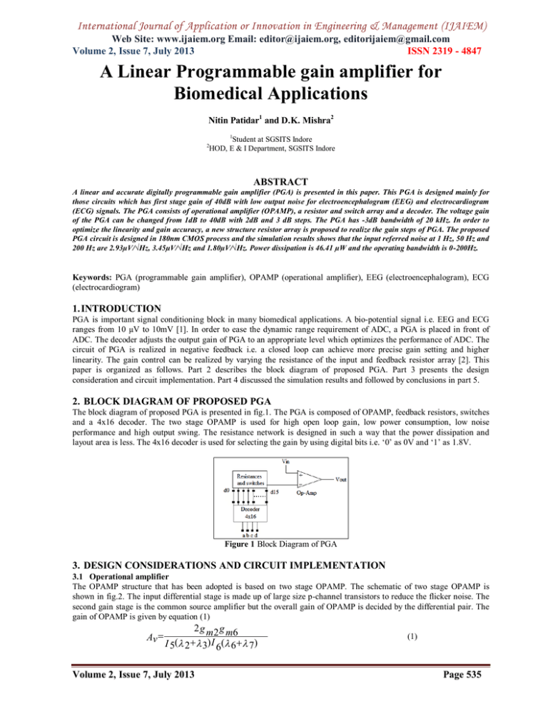
International Journal of Application or Innovation in Engineering & Management (IJAIEM) Web Site: www.ijaiem.org Email: editor@ijaiem.org, editorijaiem@gmail.com Volume 2, Issue 7, July 2013 ISSN 2319 - 4847 A Linear Programmable gain amplifier for Biomedical Applications Nitin Patidar1 and D.K. Mishra2 1 Student at SGSITS Indore HOD, E & I Department, SGSITS Indore 2 ABSTRACT A linear and accurate digitally programmable gain amplifier (PGA) is presented in this paper. This PGA is designed mainly for those circuits which has first stage gain of 40dB with low output noise for electroencephalogram (EEG) and electrocardiogram (ECG) signals. The PGA consists of operational amplifier (OPAMP), a resistor and switch array and a decoder. The voltage gain of the PGA can be changed from 1dB to 40dB with 2dB and 3 dB steps. The PGA has -3dB bandwidth of 20 kHz. In order to optimize the linearity and gain accuracy, a new structure resistor array is proposed to realize the gain steps of PGA. The proposed PGA circuit is designed in 180nm CMOS process and the simulation results shows that the input referred noise at 1 Hz, 50 Hz and 200 Hz are 2.93µV/√Hz, 3.45µV/√Hz and 1.80µV/√Hz. Power dissipation is 46.41 µW and the operating bandwidth is 0-200Hz. Keywords: PGA (programmable gain amplifier), OPAMP (operational amplifier), EEG (electroencephalogram), ECG (electrocardiogram) 1. INTRODUCTION PGA is important signal conditioning block in many biomedical applications. A bio-potential signal i.e. EEG and ECG ranges from 10 µV to 10mV [1]. In order to ease the dynamic range requirement of ADC, a PGA is placed in front of ADC. The decoder adjusts the output gain of PGA to an appropriate level which optimizes the performance of ADC. The circuit of PGA is realized in negative feedback i.e. a closed loop can achieve more precise gain setting and higher linearity. The gain control can be realized by varying the resistance of the input and feedback resistor array [2]. This paper is organized as follows. Part 2 describes the block diagram of proposed PGA. Part 3 presents the design consideration and circuit implementation. Part 4 discussed the simulation results and followed by conclusions in part 5. 2. BLOCK DIAGRAM OF PROPOSED PGA The block diagram of proposed PGA is presented in fig.1. The PGA is composed of OPAMP, feedback resistors, switches and a 4x16 decoder. The two stage OPAMP is used for high open loop gain, low power consumption, low noise performance and high output swing. The resistance network is designed in such a way that the power dissipation and layout area is less. The 4x16 decoder is used for selecting the gain by using digital bits i.e. ‘0’ as 0V and ‘1’ as 1.8V. Figure 1 Block Diagram of PGA 3. DESIGN CONSIDERATIONS AND CIRCUIT IMPLEMENTATION 3.1 Operational amplifier The OPAMP structure that has been adopted is based on two stage OPAMP. The schematic of two stage OPAMP is shown in fig.2. The input differential stage is made up of large size p-channel transistors to reduce the flicker noise. The second gain stage is the common source amplifier but the overall gain of OPAMP is decided by the differential pair. The gain of OPAMP is given by equation (1) 2 g m 2 g m6 Av I 5( 2 3) I 6( 6 7) Volume 2, Issue 7, July 2013 (1) Page 535 International Journal of Application or Innovation in Engineering & Management (IJAIEM) Web Site: www.ijaiem.org Email: editor@ijaiem.org, editorijaiem@gmail.com Volume 2, Issue 7, July 2013 ISSN 2319 - 4847 Figure 2 Two Stage CMOS Operational Amplifier The biasing voltage is provided by the series of active resistors formed by the p-channel transistors. The tail current is also generated by the p-channel transistors to reduce the noise. The n-channel current mirror load is connected to the differential pair i.e. M3 and M4. For stability of the system the Miller compensation is used and the effect of generated zero is eliminated by the nulling resistor. Table 1: Simulation results of OPAMP S.no. Specifications Simulation Results Unit 1 Gain 56.9 dB 2 Phase Margin 81 Degree 3 Gain Margin 22.25 dB 4 CMRR 67.74 dB 5 PSRR 54.4 dB 6 Power Dissipation 43.94 µW Input referred Noise At 0.5Hz 50Hz 150Hz 31.83 3.48 2.06 µV/√Hz 8 3 dB Bandwidth 20 k Hz 9 Layout Area 0.0088 mm² 10 Slew Rate 5 V/µs 11 Unity Gain Bandwidth Product 2 MHz 7 3.2 Resistance network and switches The high linear and accurate gain is achieved by using the resistor array. The proposed resistor array is formed using the floating active resistors. The advantage is being the size of transistors and low power dissipation. The resistance of floating active resistor rds is given by the equation L (2) r ds K ' W ( ) V GS V T Where, L and W are length and width of n-channel MOSFET resistor, K’ is trans-conductance parameter of same resistor, VGS is gate to source voltage and VT is the threshold voltage of n-channel MOSFET. Figure 3 Resistance and switch network Volume 2, Issue 7, July 2013 Page 536 International Journal of Application or Innovation in Engineering & Management (IJAIEM) Web Site: www.ijaiem.org Email: editor@ijaiem.org, editorijaiem@gmail.com Volume 2, Issue 7, July 2013 ISSN 2319 - 4847 The value of rds is varied from 181.7 to 23.39k to achieve the desired linear gain. The n-channel MOSFET is used as switch. The important parameters are the ron and roff. The values of ron is set to 25.69V by increasing the width of transistor and does not affect the gain linearity because it is added with the resistance of active resistor. The roff of switch is 801.6M for 20µ/180n of transistor size. Figure 4 n-channel transistor used as a switch A 4x16 decoder is used for selecting the MOSFET switches. A 4-bit input control selects the gain from 1dB to 40dB in 16 steps. Advantage of this digital control is to provide accurate output to the next stage. To implement the decoder circuit, AND gates are used. The input bits are 0V for bit ‘0’ and 1.8V for bit ‘1’. The decoder provides DC output of 1.8V to the gate of switch. Decoder design is shown in fig.5. Figure 5 A logic circuit for a 4 to 16 1-hot decoder 4. SIMULATION RESULTS The PGA is designed in 180nm CMOS process. Fig.6 shows the AC simulation of PGA for all gain settings. The PGA provides a programmable range from 1dB to 40.1dB and has -3dB bandwidth of more than 20 kHz. Fig.7 shows the curve for the PGA gain v/s digital control bits and it also shows the linearity of gain control. The simulated power dissipation of PGA is 46.41µW. the input referred noise is 2.93µV/√Hz on 40dB gain setting at 1Hz. The layout area of PGA is 0.083mm2. Table 2: Simulation results of PGA s.no Specifications . Simulation Unit Results 1 Variable Gain Range 1-40 dB 2 Power Dissipation 46.41 µW 3 Layout Area 0.083 mm² 4 Input referred Noise At 1Hz 2.93 µV/√Hz 50Hz 3.45 200Hz 1.80 5 Output Referred Noise 297.2 at 1Hz 352.9 50Hz 185.1 µV/√Hz 200Hz 6 Volume 2, Issue 7, July 2013 3 dB Bandwidth 20 kHz Page 537 International Journal of Application or Innovation in Engineering & Management (IJAIEM) Web Site: www.ijaiem.org Email: editor@ijaiem.org, editorijaiem@gmail.com Volume 2, Issue 7, July 2013 ISSN 2319 - 4847 Figure 6 Multiple gain settings of PGA 5. CONCLUSIONS This paper presents the linear and accurate programmable gain amplifier. An improved and different resistive feedback network for OPAMP is proposed to achieve accuracy and high gain linearity for PGA. The work has achieved the proposed programmable gain range with low input referred noise in desired bandwidth. The design is implemented in 180nm CMOS process with a supply of 1.8V. Figure 7 Graph showing Gain v/s Digital bits References [1.] C. C. Hsu and J. T. Wu, A highly linear 125-MHz CMOS switched-resistor programmable-gain amplifier, SolidState Circuits, IEEE Journal of, voI.38, p.I663, (2003). [2.] H. Elwan, et al., A Differential-Ramp Based 65 dB-Linear VGA Technique in 65 nm CMOS, Solid-State Circuits, IEEE Journal of, voI.44, p.2503, (2009). [3.] Woradorn Wattanapanitch and Rahul Sarpeshkar, A Low-Power 32-Channel Digitally Programmable Neural Recording Integrated Circuit, IEEE Transactions on Biomedical Circuits and Systems, vol. 5, no. 6, December 2011. [4.] Quoc-Hoang Duong, Chang-Wan Kim and Sang-Gug Lee, An 83dB Low-Power High-Linearity Variable Gain Amplifier, IEEE 2005 Custom Integrated Circuits Conference. [5.] Khaled Al-Ashmouny, Sun-Il Chang and Euisik Yoon, A 8.6 μW 3-Bit Programmable Gain Amplifier for Multiplexed-Input Neural Recording Systems, 33rd Annual International Conference of the IEEE EMBS Boston, Massachusetts USA, August 30 - September 3, 2011 AUTHOR Nitin Patidar received the B.E. degrees in Electronics and Instrumentation from IIST Indore in 2010 and M.Tech degrees in Electronics and Instrumentation from SGSITS Indore in 2013. Volume 2, Issue 7, July 2013 Page 538


