Constant-Gm, Rail-to-Rail Input Stage Operational Amplifier in 0.35μm CMOS
advertisement

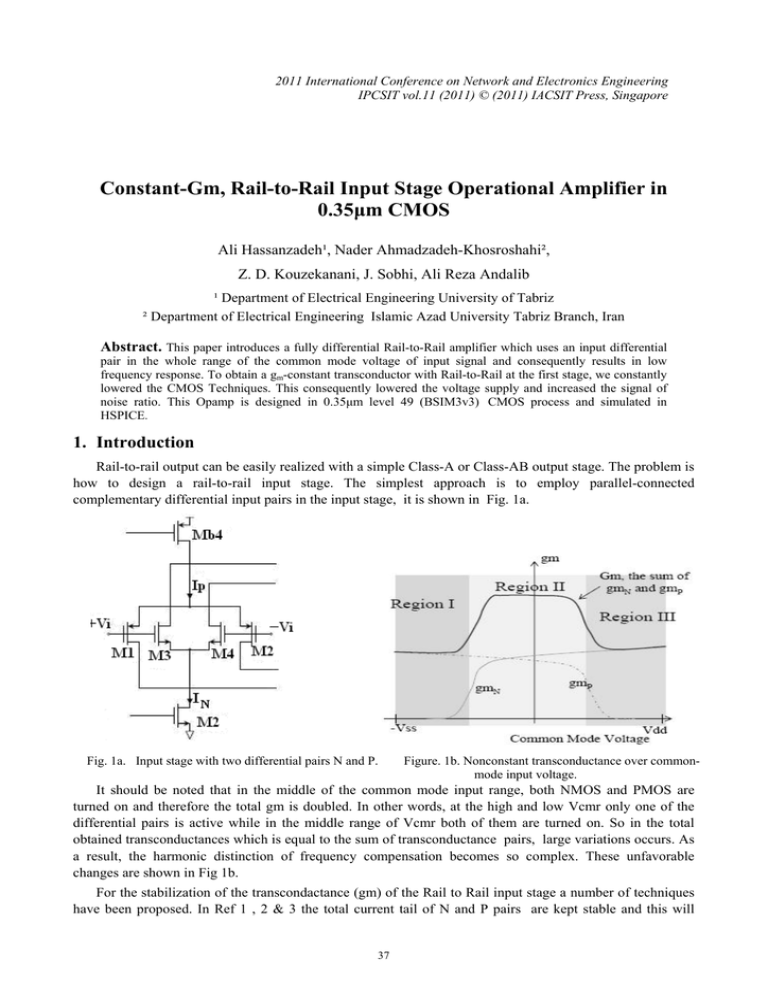
2011 International Conference on Network and Electronics Engineering IPCSIT vol.11 (2011) © (2011) IACSIT Press, Singapore Constant-Gm, Rail-to-Rail Input Stage Operational Amplifier in 0.35μm CMOS Ali Hassanzadeh¹, Nader Ahmadzadeh-Khosroshahi², Z. D. Kouzekanani, J. Sobhi, Ali Reza Andalib ¹ Department of Electrical Engineering University of Tabriz ² Department of Electrical Engineering Islamic Azad University Tabriz Branch, Iran Abstract. This paper introduces a fully differential Rail-to-Rail amplifier which uses an input differential pair in the whole range of the common mode voltage of input signal and consequently results in low frequency response. To obtain a gm-constant transconductor with Rail-to-Rail at the first stage, we constantly lowered the CMOS Techniques. This consequently lowered the voltage supply and increased the signal of noise ratio. This Opamp is designed in 0.35μm level 49 (BSIM3v3) CMOS process and simulated in HSPICE. 1. Introduction Rail-to-rail output can be easily realized with a simple Class-A or Class-AB output stage. The problem is how to design a rail-to-rail input stage. The simplest approach is to employ parallel-connected complementary differential input pairs in the input stage, it is shown in Fig. 1a. Fig. 1a. Input stage with two differential pairs N and P. Figure. 1b. Nonconstant transconductance over commonmode input voltage. It should be noted that in the middle of the common mode input range, both NMOS and PMOS are turned on and therefore the total gm is doubled. In other words, at the high and low Vcmr only one of the differential pairs is active while in the middle range of Vcmr both of them are turned on. So in the total obtained transconductances which is equal to the sum of transconductance pairs, large variations occurs. As a result, the harmonic distinction of frequency compensation becomes so complex. These unfavorable changes are shown in Fig 1b. For the stabilization of the transcondactance (gm) of the Rail to Rail input stage a number of techniques have been proposed. In Ref 1 , 2 & 3 the total current tail of N and P pairs are kept stable and this will 37 stabilizes gm. But, as we know, this method is used just when the transistors are in weak version. In Ref 4 & 5, in order to keep the current stable, the method of Squire Root biasing scheme has been offered. IP + IN Methods mentioned above are all based on squire characteristics of the MOS transistors in a saturation area. But, as we know, this assumption is not so precise for the small channel transistors. In Methods 6 and 7, also, the offered procedure requires increasing the tail current of one pair while the other pair is kept passive. (8) uses the method of current increasing of the back up pairs but it results in complicating the input stage. In (9) a simple method has been offered in which input signals are shifted but the act of shifting happen in a way that the passage areas of pairs overlap. Amplifiers of Common Drain (CD) are used here but in this circuit the frequency response is encountered with a problem since, in the input stage, a pole is included because of the CD amplifier. In this article a new structure of Rail-to-Rail input stage along with an improved frequency response (based on the shift of both of the overlapping passing areas) have been proposed. Fig. 2. Show the both transconductance shift Fig. 3 The Shifting transistor 2. The new structure of RAIL TO RAIL input As shown in Fig.2, both transconductance curves should be shifted toward each other to make their passage areas to overlap. Fig.3. We use Mn3 - Mn4 which are called Shifting transistors. These transistors are biased with stable voltage, cause to delay in working of amplifying transistors Mn1- Mn2 signal. Because of their combination they work with a high range of Vcm. To clarify the point, let’s consider the Vcm in which the shifting transistors are working while the amplifying transistors of signal are not. Thus the whole current tail passes through the shifting transistors, (Fig. 4). Fig 4. Effect of shifting transistors on tail current Fig.5 Show PMOS shifting transistor 38 By increasing Vcm at Vcm=Vnb=Vth+Vs Signal amplifying transistors on the threshold of working. Under these conditions, if we can neglect Is current of the amplifying transistors, the same (amount of) current will pass through the shifting transistor. Therefore Eq (1) : Vnb=Vthn+Vs=Vthn+Vb1-Vgs(3,4)=Vb1-(Vgd(3,4)-Vthn)=Vb1- In / K 3,4 By increasing Vcm, the current increases in the signal amplifying transistors and it decreases in the shifting transistors. In Vicm =V nc the shifting transistors are going to be off (i.e., they are approximately in the bound area where the whole current (In) passes through the amplifying transistors). (the amount of)This voltage can be calculated through the following statement: (2) Vnc=Vgs(1,2)+Vs= Vgd(1,2) + Vb1- Vthn = Vb1+ (Vgs(1,2)- Vthn) = Vb1+ In /k(1,2) As we see, in Eq (1) & (2), by the control of gmp and the size of the shifting transistors, an appropriate proportion is obtainable. In the same way we use Mp(3,4) shifting transistors to shift the gmp, (Fig.5) The amount of voltage can be calculated by the following statement: Va= Vdd+ Vthp Vb= Vthp+ Vb2 - Vgs(2,3) = Vb2- In /k(3,4) Vc = Vb2 - Ip /k(3,4) In this case, also, by the control of Vb2, K(3,4) an appropriate shift is obtainable. Changing of the shifting transistors’ size will change the passing area, (Fig. 6&7). While the changing of the Vb1 and V b2 will cause in the shifting of the passage area to the right or left, ( Fig. 8a and 8b). The size of the shifting transistors should be very small in order to obtain an appropriate overlapped passage area. By increasing the size of these transistors the passage area get linear, the act f overlapping takes place more appropriately, and the changes of the gm become less. Fig 6. Scales of calculated voltage Fig 7. Effect of changing shifting transistors' size Fig. 8a, 8b. Show voltage change in shifting transistors The folded cascade input stage causes high gained Voltage as well as well as increased output signal swing.. Considering the activeness of the two current tails in different voltages of Vcm, the current is always stable in routes 1and 2.Therefore, a large (amount of ) output signal is fixed in the whole range of Vcm .This keeps DC gained voltage stable in the whole range of Vcm ,( Fig. 9). The whole seheme of Op-amp is shown in Fig. 9. 39 Considering the differential output, we need CMFB circuit in order to stabilize Vcm output,( Fig.10). We used the "Gain Boosting Technique" to increase the DC Gain. In fact, by the use of A1 and A2 amplifiers, the output resistance of the amplifier increases to a great degree, without causing considerable changes in the frequency response. In the designing of the “helping op- amp”, we should pay much attention not to slow the response time. In the designing procedure, the main parameter to be considered is their bandwidths which should be more than the Dominant pole of the closed loop op-amp and less than the Non dominant pole of the open loop op-amp. These conditions can be simply obtained if we place C1 and C2 compensating condensers at the output of the helping op- amp. 3. The results of simulation The range of gm verification is ! .05 % . Fig . 11. Also Fig. 12. show the open loop frequency response. Capacitance of load capacitor is 2PF. As it is known, the frequency unity gain is 410 MHZ and the phase margin is 72.5 degree. The changes of the unity gain and limit angle due to Vcm is shown in Fig . 13 and 14. Figure. 15. shows the settling time of amplifying stage in unity gain feedback with Vcm =1.5. The settling time of 0.1% and 0.01% amplifier are 5/6 ns , 7.4 ns. The output swing is Vp-p = 2.8 and Vcm=1.5 Vp-p and Table.I is the list of comparision with others' works. Fig. 9. Main Schematic of OP-AMP 40 Fig. 10. Schematic of C M FB circuit Fig . 11. The range of gm verification Fig. 12. Open loop frequency response 4. CONCLUSIONS In this article a CMOS low voltage Rail- to- Rail class AB-amplifier has been proposed. The input stage of the amplifier is a Rail- to- Rail constant gm with the deviation of ±. 0.5%. In this article, also, a new input 41 stage circuit with a simple structure in which all op-amp are validated with simulation in 0.35µm CM0S technology, has been introduced. Fig. 13. Show unity gain of circuit Fig. 14. Show Phase Margin Table I. This work to previous work 5. Refrences [1] R. Hogervost, J. P. Tero, R. G. H. Eschauzier and J. H. Huijsing, “A compactpower-efficient 3-V CMOS rail-torail input/output operational amplifier for VLSI cell libraries,” IEEE Journal of Solid-State Circuits, vol. 29, no. 12, pp. [2] R. Hogervorst, S. M. Safai, and J. H. Huijsing, “A programmable 3-V CMOS rail-to-rail opamp with gain boosting for driving heavy loads,” IEEE Proc. ISCAS1995, pp. 1544-1547. [3] J. H. Huijsing, R. Hogervorst, and K.-J. de Langen, “Low-power low-voltageVLSI operational amplifier cells,” IEEE Trans. Circuits and Systems-I, vol. 42. no.11, pp. 841-852, November 1995. [4] S. Sakurai and M. Ismail, “Robust design of rail-to-rail CMOS operationalamplifiers for a low power supply voltage,” IEEE Journal of Solid-State Circuits,vol. 31, no. 2, pp. 146-156, February 1996. [5] J. H. Botma, R. F. Wassenaar, and R. J. Wiegerink, “A low voltage CMOS op amp with a rail-to-rail constant-gm input stage and a class AB rail-to-rail output stage, ”IEEE Proc. ISCAS 1993, vol. 2, pp. 1314-1317, May 1993. [6] C. Hwang, A. Motamed, and M. Ismail, “LV opamp with programmable rail-to-rail constant-gm,” IEEE Proc. 1997 [7] C. Hwang, A. Motamed, and M. Ismail, “Universal constant-gm input-stage architecture for low-voltage op amps,” IEEE Trans. Circuits and Systems-I, vol.42. no. 11, pp. 886-895, November 1995. [8] W. Redman-White, “A high bandwidth constant gm, and slew-rate rail-to-rail CMOS input circuit and its application to analog cell for low voltage VLSI systems,” IEEE Journal of Solid-State Circuits, vol. 32, no. 5, pp. 701-712, May 1997. 42 [9] M. Wang, T.L. Mayhugh, S.H.K. Embabi, and E. Sanchez-Sinencio, “Constant-gm Rail-to-Rail CMOS Op-Amp Input Stage with Overlapped Transition Regions ,” IEEE J. of Solid State Circuits, vol. 34, no. 2, pp. 148-156, Feb. 1999. [10] Mohammad Mehdi Ahmadi , "An Adaptive Biased Single-Stage CMOS Operational Amplifier with a Novel [11] Rail-to-Rail Constant-gm Input Stage" Analog Integrated Circuits and Signal Processing, 45, 71–78, 2005 [12] Pujitha Weerakoon Frederick J. Sigworth Peter J. Kindlmann Eugenio Culurciello "rail-to-rail operational amplifier [13] in silicon-on-sapphire with constant transconductance" Analog Integr Circ Sig Process (2010) 65:311–319 springer 43


