Simulation of Carbon Nanotube with Phonon Scattering
advertisement
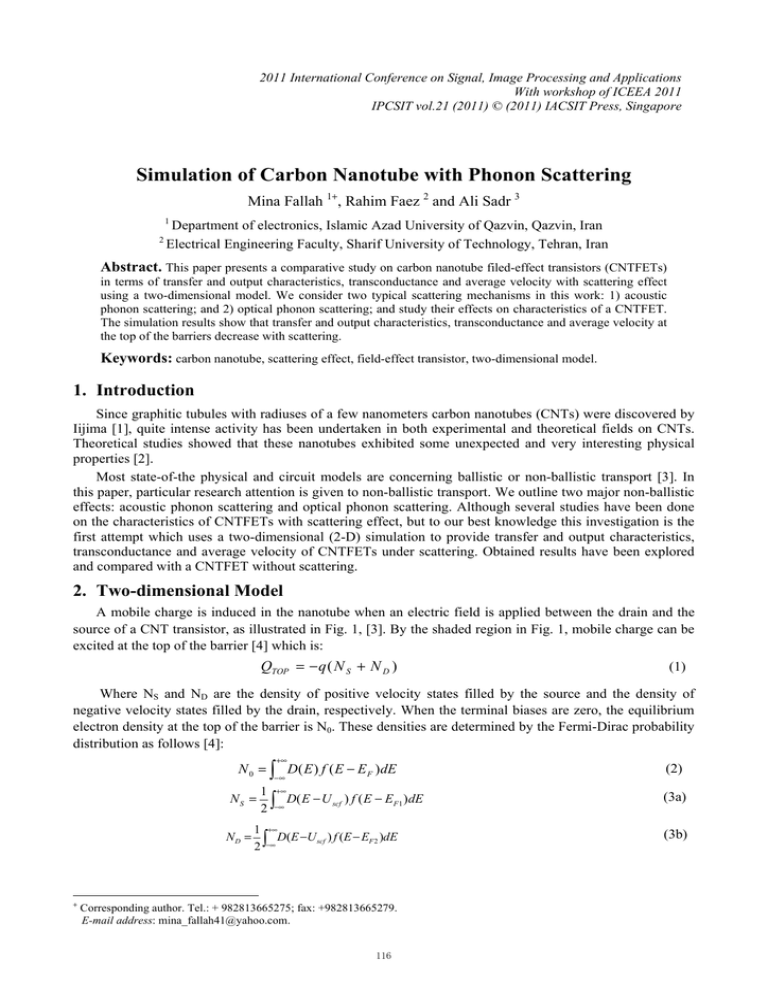
2011 International Conference on Signal, Image Processing and Applications With workshop of ICEEA 2011 IPCSIT vol.21 (2011) © (2011) IACSIT Press, Singapore Simulation of Carbon Nanotube with Phonon Scattering Mina Fallah 1+, Rahim Faez 2 and Ali Sadr 3 1 2 Department of electronics, Islamic Azad University of Qazvin, Qazvin, Iran Electrical Engineering Faculty, Sharif University of Technology, Tehran, Iran Abstract. This paper presents a comparative study on carbon nanotube filed-effect transistors (CNTFETs) in terms of transfer and output characteristics, transconductance and average velocity with scattering effect using a two-dimensional model. We consider two typical scattering mechanisms in this work: 1) acoustic phonon scattering; and 2) optical phonon scattering; and study their effects on characteristics of a CNTFET. The simulation results show that transfer and output characteristics, transconductance and average velocity at the top of the barriers decrease with scattering. Keywords: carbon nanotube, scattering effect, field-effect transistor, two-dimensional model. 1. Introduction Since graphitic tubules with radiuses of a few nanometers carbon nanotubes (CNTs) were discovered by Iijima [1], quite intense activity has been undertaken in both experimental and theoretical fields on CNTs. Theoretical studies showed that these nanotubes exhibited some unexpected and very interesting physical properties [2]. Most state-of-the physical and circuit models are concerning ballistic or non-ballistic transport [3]. In this paper, particular research attention is given to non-ballistic transport. We outline two major non-ballistic effects: acoustic phonon scattering and optical phonon scattering. Although several studies have been done on the characteristics of CNTFETs with scattering effect, but to our best knowledge this investigation is the first attempt which uses a two-dimensional (2-D) simulation to provide transfer and output characteristics, transconductance and average velocity of CNTFETs under scattering. Obtained results have been explored and compared with a CNTFET without scattering. 2. Two-dimensional Model A mobile charge is induced in the nanotube when an electric field is applied between the drain and the source of a CNT transistor, as illustrated in Fig. 1, [3]. By the shaded region in Fig. 1, mobile charge can be excited at the top of the barrier [4] which is: QTOP = − q ( N S + N D ) (1) Where NS and ND are the density of positive velocity states filled by the source and the density of negative velocity states filled by the drain, respectively. When the terminal biases are zero, the equilibrium electron density at the top of the barrier is N0. These densities are determined by the Fermi-Dirac probability distribution as follows [4]: +∞ N 0 = ∫ D( E ) f ( E − E F )dE −∞ NS = ND = + 1 +∞ D( E − U scf ) f ( E − EF 1 )dE 2 ∫−∞ 1 +∞ D(E −U scf ) f (E − EF 2 )dE 2 ∫−∞ Corresponding author. Tel.: + 982813665275; fax: +982813665279. E-mail address: mina_fallah41@yahoo.com. 116 (2) (3a) (3b) Where D(E) is the density of states at the top of the barrier, Uscf is the self-consistent voltage at the top of the barrier, EF is the Fermi level, ƒ is the equilibrium Fermi function and E represents the energy levels, EF1=EF and EF2=EF -qVDS are source and drain Fermi levels. Fig. 1: Two-dimensional circuit model for transistors. It consists of three capacitors, which represent the effect of three terminals on the potential at the top of the barrier. The potential at the top of the barrier, Uscf, is controlled by the gate, drain and source potentials. The mobile charge at the top of the barrier is determined by Uscf and by the location of the two Fermi levels EF1 and EF2 [4]. When density of states D(E) and the location of the source and drain Fermi levels is define, we can evaluate the electron density at the top of the barrier, N=NS+ND, if the self-consistent potential is known [4]. The self-consistent voltage Uscf can be calculated in two parts as bellow [4, 5]: i) Ignoring the presence of the mobile charge in the channel and calculating the Laplace potential at the top of the barrier due to terminal biases leads to: U L = − q (α GVG + α DV D + α S V S ) (4a) In the above equation αG, αD and αS describe how the gate, drain and source control the Laplace solution and can be written as: C C C (4b) αG = G α D = D α S = S CΣ CΣ CΣ Where CΣ is the parallel combination of the three capacitors in Fig. 1. ii) The second part of the solution consists of grounding the three terminals and computing the potential due to the change of mobile charge at the top of the barrier, ΔN= (NS+ND)-N0, from UP = q2 ΔN CΣ (5) The complete solution is obtained by adding the two contributions U scf = U L + U P = −q(α GVG + α DVD + α SVS ) + U P (6) Equations (3a), (3b) and (6) represent two coupled nonlinear equations for the two unknowns N and Uscf. The iteration between these equations continues until the carrier density and self-consistent potential at the top of the barrier. After the self-consistency is achieved the current is given according to the following formula: +∞ I D = ∫ J ( E − U scf )[ f ( E − E F 1 ) − f ( E − E F 2 )]dE −∞ (7a) Where J(E_ Uscf) is the ‘‘current-density-of-states’’, which is expressed as J ( E − U scf ) = 1 ⎛⎜ 2 q 2 ⎜⎝ π 2( E − U scf ) ⎞ ⎟ D( E − U scf ) ⎟ m* ⎠ (7b) 3. Results and Discussion In this section, first we have simulated a CNTFET with a 1.5 nm thick gate oxide and the relative dielectric constant εr=3.9 while the channel is a (17, 0) nanotube (see Fig. 2). Then, we entered the scattering effect in this CNTFET. Our simulations are in agreement with the results reported in [3, 5]. 117 Fig. 2: Cross-sectional view of a coaxial CNTFET [6]. 3.1. Phonon scattering For semiconducting carbon nanotubes, the phonon scattering depend on the carrier energy and influences on the current of a CNTFET. The effective phonon scattering mean free path (MFP) in a semiconducting nanotube can be computed by [6] 1 1 1 = + l sc (V x ) lap (V x ) lop (V x ) (8) Where lap and lop are the effective acoustic phonon scattering MFP and the effective optical phonon scattering MFP respectively and are obtained from l ap (V x ) = lop (V x ) = λ ap Do D ( E )[1 − D ( E )[1 − (9a) 1 ] ( E F −U scf + qV x ) e λop Do (9b) 1 e ( E F − = Ω − U scf + qV x ) ] In this equation, λap ≈ 500nm is a typical acoustic phonon scattering MFP, λop ≈ 15nm is a typical optical phonon scattering MFP and ћΩ ≈ 0.16eV is a optical phonon energy. Do is a constant 8/(3πVπacc), where acc and Vcc are the carbon π – π nearest-neighbor bond length and energy of the tight bonding model respectively. Thus, for a CNTFET, the scattering effect current can be obtained using I DSP 2qkT = [T ln(1 + e π= LR EF −U scf kT EF −U scf − qVDS ) − TRL ln(1 + e kT )] (10) Where TLR and TRL are the transmission probabilities and are given by TLR = lsc (VDS ) lsc (VDS ) + Lg TLR = lsc (VDS ) lsc (VDS ) + Lg (11a) (11b) We compared this CNTFET in terms of transfer and output characteristics, transconductance and average velocity with a CNTFET without scattering. 118 (a) (b) Fig. 3: (a) Transfer characteristics under both low and high drain bias without and with scattering effect, (b) Output characteristics without and with scattering effect. Fig. 3 shows an accuracy comparison in transfer and output characteristics between CNTFET without and with scattering effect. The transconductance (gm) is extracted from the slope of ID-VGS at VDS = 0.6. As can be seen in Fig. 4a, the scattering effect causes the transconductance decreases. The average electron velocity at the top of the barrier increases with VDS and then saturates. Saturation of velocity occurs in a ballistic transistor, but it occurs at the top of the barrier where the field is zero, rather than at the drain end where the field is high [4]. The carrier velocity is expressed as ν = I D (VGS , VDS ) Q(VGS , VDS ) (12a) Thus the average velocity of carrier at top of the barrier can be defined as: ν = I D (VGS , VDS ) − q[ N S (VGS , VDS ) + N D (VGS , VDS )] Fig. 4b presents, the average velocity of carrier decreases under scattering effect condition. 119 (12b) (a) (b) Fig. 4: (a) Transconductance versus the gate voltage without and with scattering effect, (b) Average velocity versus the gate voltage without and with scattering effect. 4. Conclusion In this paper, we presented a comparative study on carbon nanotube filed-effect transistors (CNTFETs) in terms of transfer and output characteristics, transconductance and average velocity with acoustic and optical scattering effects using a two-dimensional model. The simulation results show that transfer and output characteristics, transconductance and average velocity at the top of the barriers decrease with scattering. 5. References [1] S. Iijima, “Helical microtubules of graphitic carbon,” Nature Publishing Group, vol. 354, pp. 56 –58, November, 1991. [2] L. Yang, M. P. Anantram, Jie _ Han, and J. P. Lu, “Band-gap change of carbon nanotubes: Effect of small uniaxial and torsional strain,” Physical Review Letters, vol. 60, no. 19, pp. 13874–13878, November, 1999. [3] T.Kazmierski, D. Zhou, B. M. Al-Hashimi and P. Ashburn, Numerically efficient modeling of CNT transistors with ballistic and non-ballistic effects for circuit simulation, IEEE Trans, pp. 1-9, 2009. [4] A. Rahman, J. Guo, S. Datta and M. S. Lundstrom, Theory of ballistic nanotransistors, Electron Devices, IEEE Transactions on Electron Devices, vol. 50, no. 9, pp. 1853–1864, September, 2003. [5] Z. Arefinia, Ali A. Orouji, Investigation of the novel attributes of a carbon nanotube FET with high-k gate dielectrics. Physica E, vol. 40, pp. 3068–3071, April, 2008. [6] J. Deng and H.S.Philip Wong, A compact spice model for carbon nanotube field-effect transistors including non idealities and its application- part i: model of the intrinsic channel region, IEEE Transactions on Electron Devices, vol. 54, no. 12, pp. 3195–3205, December, 2007. 120
