Document 13127564
advertisement
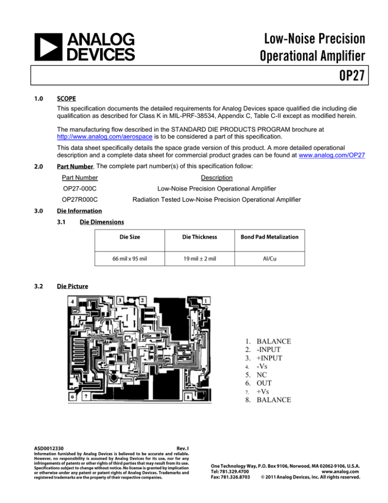
This specification documents the detailed requirements for Analog Devices space qualified die including die qualification as described for Class K in MIL-PRF-38534, Appendix C, Table C-II except as modified herein. The manufacturing flow described in the STANDARD DIE PRODUCTS PROGRAM brochure at http://www.analog.com/aerospace is to be considered a part of this specification. This data sheet specifically details the space grade version of this product. A more detailed operational description and a complete data sheet for commercial product grades can be found at www.analog.com/OP27 The complete part number(s) of this specification follow: Part Number Description OP27-000C Low-Noise Precision Operational Amplifier OP27R000C Radiation Tested Low-Noise Precision Operational Amplifier 1. BALANCE 2. -INPUT 3. +INPUT 4. -VS 5. NC 6. OUT 7. +VS 8. BALANCE Supply Voltage (VS) ................................................................. ±22V Input Voltage 2/ ......................................................................... ±22V Output Short Circuit Duration .................................................... Indefinite Differential Input Voltage 3/ ........................................................ ±0.7V Differential Input Current 3/ ........................................................ ±25mA Storage Temperature Range ................................................... -65C to +150C Operating Temperature Range ................................................... -55C to +125C Junction Temperature (TJ)………………………………..………... 150°C Absolute Maximum Ratings Notes 1/ Stresses above the absolute maximum rating may cause permanent damage to the device. Extended operation at the maximum levels may degrade performance and affect reliability. 2/ For supply voltages less than ±22V, the absolute maximum input voltage is equal to the supply voltages. 3/ The device inputs are protected by back-to-back diodes. Current limiting resistors are not used in order to achieve low noise. If differential input voltage exceeds ±0.7V, the input current should be limited to 25mA. In accordance with class-K version of MIL-PRF-38534, Appendix C, Table C-II, except as modified herein. (a) Qual Sample Size and Qual Acceptance Criteria – 10/0 (b) Qual Sample Package – DIP (c) Pre-screen electrical test over temperature performed post-assembly prior to die qualification. Table I Notes: 1/ VS = ±15V, TA = 25C, unless otherwise specified. Table II Notes: 1/ 2/ 3/ VS = ±15V, RS = 50, unless otherwise specified. This parameter not tested post irradiation. Devices tested at 100Krad irradiation. 5.1 5.2 5.3 HTRB is not applicable for this drawing. Burn-in is per MIL-STD-883 Method 1015 test condition B or C. Steady state life test is per MIL-STD-883 Method 1005.
