Document 13127546
advertisement
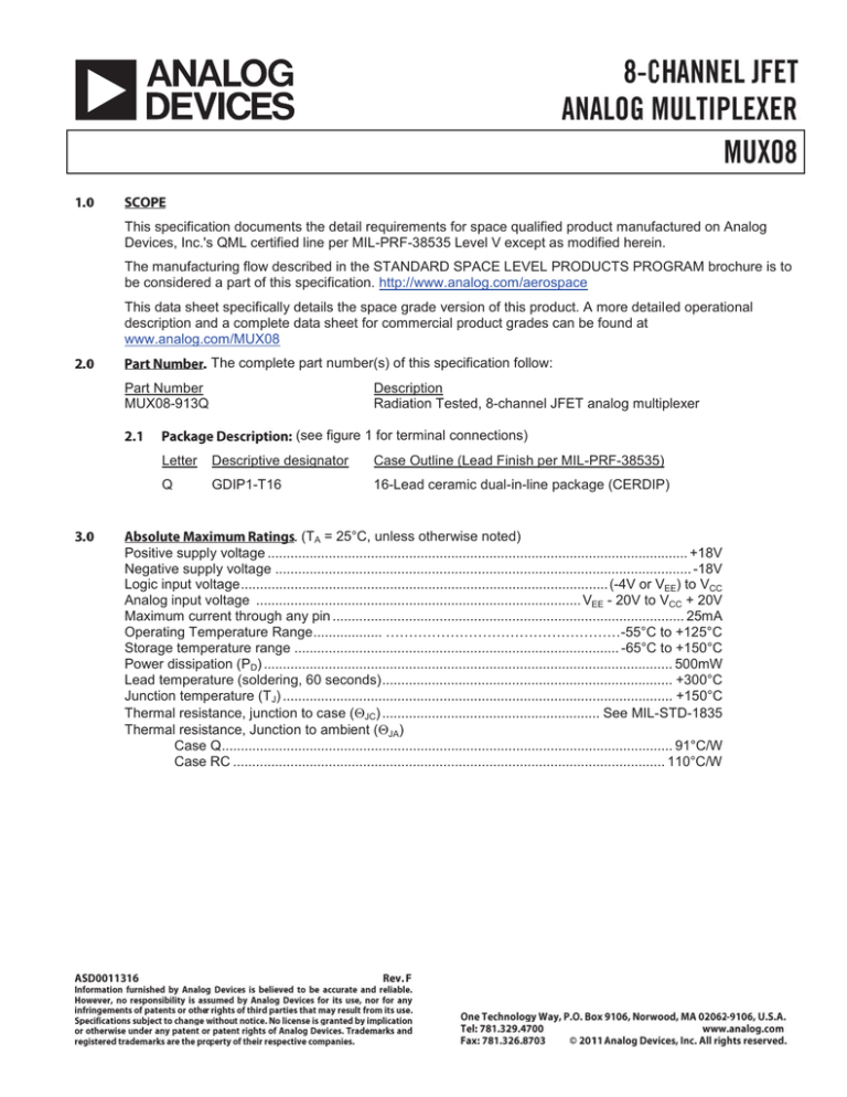
This specification documents the detail requirements for space qualified product manufactured on Analog Devices, Inc.'s QML certified line per MIL-PRF-38535 Level V except as modified herein. The manufacturing flow described in the STANDARD SPACE LEVEL PRODUCTS PROGRAM brochure is to be considered a part of this specification. http://www.analog.com/aerospace This data sheet specifically details the space grade version of this product. A more detailed operational description and a complete data sheet for commercial product grades can be found at www.analog.com/MUX08 The complete part number(s) of this specification follow: Part Number MUX08-913Q Description Radiation Tested, 8-channel JFET analog multiplexer (see figure 1 for terminal connections) Letter Descriptive designator Case Outline (Lead Finish per MIL-PRF-38535) Q GDIP1-T16 16-Lead ceramic dual-in-line package (CERDIP) (TA = 25°C, unless otherwise noted) Positive supply voltage .............................................................................................................. +18V Negative supply voltage ............................................................................................................. -18V Logic input voltage ................................................................................................ (-4V or VEE) to VCC Analog input voltage ..................................................................................... VEE - 20V to VCC + 20V Maximum current through any pin ............................................................................................ 25mA Operating Temperature Range .................. ……………………………………………-55°C to +125°C Storage temperature range ..................................................................................... -65°C to +150°C Power dissipation (PD) ........................................................................................................... 500mW Lead temperature (soldering, 60 seconds) ............................................................................ +300°C Junction temperature (TJ) ...................................................................................................... +150°C Thermal resistance, junction to case (4JC) ......................................................... See MIL-STD-1835 Thermal resistance, Junction to ambient (4JA) Case Q...................................................................................................................... 91°C/W Case RC ................................................................................................................. 110°C/W Figure 1 - Terminal connections. Figure 2 - Truth Table P P ' : P ' P P : : TABLE I NOTES: Guaranteed, if not tested, to the specified limits 1/ Verified by leakage tests 2/ Conditions applied to leakage tests insure worst case leakages. 3/ 4/ RON MATCH specified as a percentage of RAVERAGE where: 1 N with N = number of channels, Ri = each channel's "ON" resistance. R AVERAGE N ¦ Ri i 1 1/ 2/ PDA applies to Subgroup 1 only. Delta limits are excluded from PDA See table III for delta limits. 5.1 5.2 5.3 HTRB is not applicable for this drawing. Burn-in is per MIL-STD-883 Method 1015 test condition B. Steady state life test is per MIL-STD-883 Method 1005. Figure 4 - Transition time test circuit Figure 5 - Switching time waveforms Figure 6 - Enable delay time test circuit Figure 7 - Break-before-make test circuit

