Solid-state detectors: A new approach to thermal neutron detection
advertisement

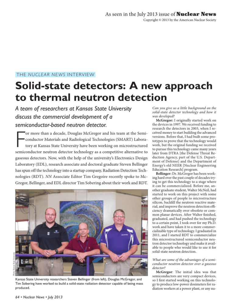
As seen in the July 2013 issue of Nuclear News Copyright © 2013 by the American Nuclear Society T H E N U C L E A R N E W S I N T E RV I E W Solid-state detectors: A new approach to thermal neutron detection A team of researchers at Kansas State University discuss the commercial development of a semiconductor-based neutron detector. F Photo: Kansas State University or more than a decade, Douglas McGregor and his team at the Semiconductor Materials and Radiological Technologies (SMART) Laboratory at Kansas State University have been working on microstructured semiconductor neutron detector technology as a competitive alternative to gaseous detectors. Now, with the help of the university’s Electronics Design Laboratory (EDL), research associate and doctoral graduate Steven Bellinger has spun off the technology into a startup company, Radiation Detection Technologies (RDT). NN Associate Editor Tim Gregoire recently spoke to McGregor, Bellinger, and EDL director Tim Sobering about their work and RDT. Kansas State University researchers Steven Bellinger (from left), Douglas McGregor, and Tim Sobering have worked to build a solid-state radiation detector capable of being mass produced. 64 • Nuclear News • July 2013 Can you give us a little background on the solid-state detector technology and how it was developed? McGregor: I originally started work on the devices in 1997. We received funding to research the detectors in 2003, when I received money to start building the advanced versions. Before that, I had built some prototypes to prove that the technology would work, but the original funding we received to pursue this technology came many years later from DTRA [the Defense Threat Reduction Agency, part of the U.S. Department of Defense] and the Department of Energy’s old NEER [Nuclear Engineering Education Research] program. Bellinger: Dr. McGregor has been working hard over the past couple of decades trying to get this technology to a stage where it can be commercialized. Before me, another graduate student, Walter McNeil, had started to work on this project with some other groups of people to microstructure silicon, backfill the neutron reactive material, and improve the neutron detection efficiency dramatically over obsolete or common planar devices. After Walter finished, graduated, and had pushed the technology to a certain point, I took over for my Ph.D. work and have taken it to a more commercializable type of technology. I graduated in 2011, and I started RDT to commercialize this microstructured semiconductor neutron detector technology and make it available to people who would like to use it for solid-state neutron detection. What are some of the advantages of a semiconductor neutron detector over a gaseous detector? McGregor: The initial idea was that semiconductors are very compact devices, so I first started working on this technology to produce low-power dosimeters for radiation workers at a power plant, or any nu- clear facility, who handle neutron sources. So those were the immediate pluses: They are compact and can be operated on low power. The detectors operate on only 2 or 3 volts, so we don’t need much power to run them. It turns out that there’s more to it, though. We can pack them in moderators, where we can also measure fast neutrons. We’re making detectors now that compete with the same efficiency as helium-3 gasfilled detectors. The one difference is that helium-3 detectors operate on hundreds to thousands of volts, whereas our detectors, as I said, operate on only a few volts. Another advantage is that the detectors can be mass produced in a laboratory in much the same manner as silicon chips that you might buy at a common store, like Radio Shack. Although I don’t expect to see Steven is now sending out to customers. The detectors come with their own electronics, which were designed in the Electronics Design Laboratory, and all of the detectors have been fabricated in the SMART Laboratory at Kansas State. The entire device, with preamplifier, is all one unit, and each one is about 1-inch square in size. Can you explain the process used for etching and backfilling the semiconductors? McGregor: I can explain both the philosophy and the process. When we undertook the project, it was very clear to us that our sponsors, mainly DTRA, wanted us to produce something that would not be a prototype that was difficult to build or reproduce. Instead, the goal was to make something that could be mass produced. So we approached the problem with the end goal in mind of making a simplified process where we could, in fact, make hundreds or thousands of these detectors per batch. The students working with me, including Steven, worked on methods of simplifying the process so that we could mass produce them. In other words, it is one thing to go into a laboratory and make one detector that works well, but it’s a completely different matter to create a process that’s repeatable over and over with high-yield success. So that’s what we’ve done. The process we use to etch the detectors has been modified to where we use a special orientation of silicon wafers, in which the wafers are dipped in a potassium hydroxide solution, and that is used to etch these oriented trenches deep into the wafer. The wafers are oriented one-one-zero [Miller indices (110)] on the surface, and that’s important because it allows Steven to etch trenches almost all the way through a wafer, which is on the order of 600 to 700 microns thick, in a matter of hours. That process is much faster than what any plasma etching system can do, and he can perform the etch for 25 wafers at a time, so they are batch processed. The other issue I was confronted with was how to backfill those trenches with a material that is neutron sensitive. We had a lot of skeptics telling us that this was going to be the main problem. But it was Steven who came up with a very creative and innovative way of doing it, which we’ve kept kind of secret up until now. We use a colloidal solution of lithium fluoride, which we push down into the crevices using a centrifuge. “It is one thing to go into a laboratory and make one detector that works well, but it’s a completely different matter to create a process that’s repeatable over and over with high-yield success. So that’s what we’ve done.” these detectors at Radio Shack, we do use the same type of technology to produce the detectors as is needed to fabricate common transistors. Steven has the ability to make hundreds of detectors per run, and per unit area they can compete fairly well with helium-3 detectors. Bellinger: Also, I don’t want to leave out the electronics that we’ve developed with EDL, and Tim can speak on that. Sobering: With EDL, Kansas State is unique in that we set it up so that the researchers can focus on the technology they’re developing, and we’ve built an umbrella around them with professional engineers who can work with them on developing the electronics. We’ve actually pushed this to a very low-power, very low-voltage operation—a very compact package—by working nearly every day with Dr. McGregor, Walter, and now Steven, trading off all of the problems and issues that come up. By having that captive capability, it makes Kansas State pretty unique in both the research side and being able to spin this off as a commercial entity, because they essentially have a packaged, ready-to-sell product now. McGregor: That’s absolutely correct. The technology has gone from the drawing board, literally, to a compact package that And it takes a matter of 10 to 15 minutes to do that. So with these two processes— rapidly etching the trenches in the solution and then backfilling those trenches with a centrifuge—we can now mass produce these detectors at a very low cost. Those are the two major processes that differ from traditional semiconductor processing, while the rest of the steps are typical processes used to make diodes and so forth in a clean room. What was EDL’s role in developing the detector interface? Sobering: We’ve been developing the preamplifier and other associated electronics for years now, and the challenge has been that as Dr. McGregor and his group have encountered various issues that come up with this processing, because the diodes are unique, we’ve had to adapt the electronics and customize them to compensate for some of the behavior while preserving the lowpower operation. So it’s been a partnership with my lab, and we’ve gone through a number of different versions as things have changed and efficiencies have increased to get to the point where we are today. How does it work? Sobering: It depends on how you’re planning to apply the device. But let’s take, for example, the dosimeter application, in which case you’re simply counting neutron events. We want that to be specific to neutrons and work to reject the gamma, and obviously Steven and Dr. McGregor are the ones to talk about that side of things. What I’m providing is a low-noise, low-power preamplifier with a shaper component, and then all of the biasing and thresholding circuitry to give them an output that is compatible with a counting system. What is the neutron detection efficiency achieved by the detectors? Bellinger: Currently, RDT has, more or less, pushed the technology to where we can pretty reasonably and easily reproduce 20 to 25 percent thermal neutron detection efficiency devices. After that, it will take some further engineering to go beyond 30 percent or so for the device itself. McGregor: So far the best we’ve done with measuring detector efficiency is 42 percent from a single device, and Steven built that device. The theoretical limit that we’re seeing right now with a new design that I have on the table, and which we’ll hopefully be building next year, will allow us to reach 70 percent thermal neutron detection efficiency. And that’s the intrinsic efficiency. So 70 percent becomes quite interesting, and that number is for a single device. We look forward to making those new detectors in the near future. Now, as far as gamma-ray discrimination is concerned, the design of the detector allows us to reach a higher discrimination ra- July 2013 • Nuclear News • 65 Photo: KSU SMART Lab/RDT Solid-State Detectors: A New Approach to Thermal Neutron Detection A scanning electron microscope image of the microstructured semiconductor reveals the trenches backfilled with neutron reactive lithium-6 fluoride. tio than you would with a coated-type neutron detector, for instance, a gas tube that may be coated with boron or lithium fluoride. The discrimination ratio is also better than the older formatted semiconductor neutron detectors, where a neutron reactive coating is simply laid upon a diode. The trenches do more than just increase the surface area and the amount of material that neutrons interact with. They also serve to change the way the output spectrum appears. The way we design these detectors—and I don’t want to go into detail here as to why this physically happens—allows us to have a large dip in the pulse-height spectrum near the noise level, where we can discriminate out the background. This important feature does not appear in other permutations of the microstructured design, so we’re very careful to design that dip feature into the detectors. And by engineering that design feature into the detectors, we can get gamma-ray discrimination ratios on the order of 108 neutrons to one gamma-ray, so it’s actually a couple of orders of magnitude higher than what you can achieve with a helium-3 tube. You talked about the use of the detectors as dosimeters. What other possible applications do you see them being used for? Bellinger: A lot of what RDT is focusing on is compact, low-power applications. Some of the applications may include the monitoring of radioactive waste materials, or specifically, maybe mounting on UAVs [unmanned aerial vehicles] for lightweight neutron detectors, or gamma detectors for other technologies that RDT is considering. So a lot of the applications we see, at least for this technology, are for compact, lowpower applications. Sobering: Which then gives you longterm monitoring capability for potentially remote, battery-operated applications. You 66 • Nuclear News • July 2013 have a much higher capability of watching something over long periods of time with this kind of technology. McGregor: Certainly there was the initial idea of dosimetry, but we also made reach-back dosimeters. In other words, they were radio controlled, and you could read them from a distance. That’s something that we have built prototypes of already. Oil well logging comes to mind. And survey meters—these detectors would be an interesting attachment to survey meters. It would be a pretty simple attachment. These neutron detectors might serve any application that you can think of where a compact neutron detector might be of use. Especially with the increased cost of helium-3 gas, you can imagine that there are many other roles that these detectors may take over as we continue to develop them. What is RDT’s current production capacity? Bellinger: Currently, production capacity is limited by the orders that come in. But if we were to say that we had to go full scale on the orders, then it would be easy to process perhaps on the order of 100 to 500 wafers per month, which would each have at least 10 devices on them. So we’re looking at 1000 to 5000 detectors per month at full-scale production. Now, some of the limitations come from human resources, but that can be upgraded, and we can hire people to handle some of those problems. What Dr. McGregor has here at Kansas State’s SMART Lab is a small to medium-sized production-scale semiconductor facility, so quite a bit of the work can be initially commercialized through that production facility. At the point where we reach a higher number of sales, production could be farmed out to other semiconductor facilities, or RDT could build its own highcapacity production facility.


