FPGA based Ternary Content Addressable Memory using SRAM Preeti Singh , Rajesh Mehra
advertisement
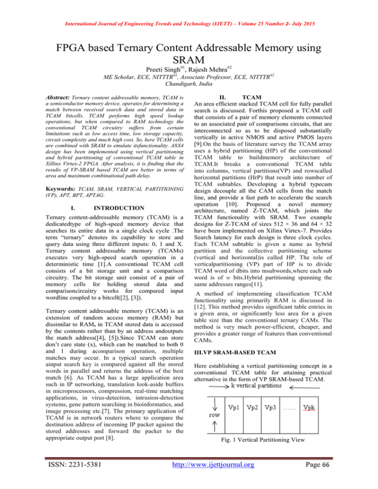
International Journal of Engineering Trends and Technology (IJETT) – Volume 25 Number 2- July 2015 FPGA based Ternary Content Addressable Memory using SRAM Preeti Singh#1, Rajesh Mehra#2 ME Scholar, ECE, NITTTR#1, Associate Professor, ECE, NITTTR#2 Chandigarh, India Abstract: Ternary content addressable memory, TCAM is a semiconductor memory device, operates for determining a match between received search data and stored data in TCAM bitcells. TCAM performs high speed lookup operations, but when compared to RAM technology the conventional TCAM circuitry suffers from certain limitations such as low access time, low storage capacity, circuit complexity and much high cost. So, here TCAM cells are combined with SRAM to emulate itsfunctionality. A8X4 design has been implemented using vertical partitioning and hybrid partitioning of conventional TCAM table in Xillinx Virtex-2 FPGA. After analysis, it is finding that the results of VP-SRAM based TCAM are better in terms of area and maximum combinational path delay. Keywords: TCAM, SRAM, VERTICAL PARTITIONING (VP), APT, BPT, APTAG. I. INTRODUCTION Ternary content-addressable memory (TCAM) is a dedicatedtype of high-speed memory device that searches its entire data in a single clock cycle .The term “ternary” denotes its capability to store and query data using three different inputs: 0, 1 and X. Ternary content addressable memory (TCAMs) executes very high-speed search operation in a deterministic time [1].A conventional TCAM cell consists of a bit storage unit and a comparison circuitry. The bit storage unit consist of a pair of memory cells for holding stored data and comparisoncircuitry works for compared input wordline coupled to a bitcell([2], [3]). Ternary content addressable memory (TCAM) is an extension of random access memory (RAM) but dissimilar to RAM, in TCAM stored data is accessed by the contents rather than by an address andoutputs the match address([4], [5]).Since TCAM can store don‟t care state (x), which can be matched to both 0 and 1 during acomparison operation, multiple matches may occur. In a typical search operation ainput search key is compared against all the stored words in parallel and returns the address of the best match [6]. As TCAM has a large application area such in IP networking, translation look-aside buffers in microprocessors, compression, real-time matching applications, in virus-detection, intrusion-detection systems, gene pattern searching in bioinformatics, and image processing etc.[7]. The primary application of TCAM is in network routers where to compare the destination address of incoming IP packet against the stored addresses and forward the packet to the appropriate output port [8]. ISSN: 2231-5381 II. TCAM An area efficient stacked TCAM cell for fully parallel search is discussed. Forthis proposed a TCAM cell that consists of a pair of memory elements connected to an associated pair of comparisons circuits, that are interconnected so as to be disposed substantially vertically in active NMOS and active PMOS layers [9].On the basis of literature survey the TCAM array uses a hybrid partitioning (HP) of the conventional TCAM table to buildmemory architecture of TCAM.It breaks a conventional TCAM table into columns, vertical partitions(VP) and rowscalled horizontal partitions (HrP) that result into number of TCAM subtables. Developing a hybrid typecam design decouple all the CAM cells from the match line, and provide a fast path to accelerate the search operation [10]. Proposed a novel memory architecture, named Z-TCAM, which joints the TCAM functionality with SRAM. Two example designs for Z-TCAM of sizes 512 × 36 and 64 × 32 have been implemented on Xilinx Virtex-7. Provides Search latency for each design is three clock cycles. Each TCAM subtable is given a name as hybrid partition and the collective partitioning scheme (vertical and horizontal)is called HP. The role of verticalpartitioning (VP) part of HP is to divide TCAM word of dbits into msubwords,where each sub word is of w bits.Hybrid partitioning spanning the same addresses ranges[11]. A method of implementing classification TCAM functionality using primarily RAM is discussed in [12]. This method provides significant table entries in a given area, or significantly less area for a given table size than the conventional ternary CAMs. The method is very much power-efficient, cheaper, and provides a greater range of features than conventional CAMs. III.VP SRAM-BASED TCAM Here establishing a vertical partitioning concept in a conventional TCAM table for attaining practical alternative in the form of VP SRAM-based TCAM. Fig. 1 Vertical Partitioning View http://www.ijettjournal.org Page 66 International Journal of Engineering Trends and Technology (IJETT) – Volume 25 Number 2- July 2015 Vertical partitioning logically dissects a conventional TCAM table column-wise into „k‟ number of TCAM sub-tables. These TCAM sub tables are then processed to be stored in their correspondingSRAM blocks. Vertical partitioning implies that a TCAM word of width „W‟ bits are divided into „k‟ subwords, each of which is of width „w‟ bits.Fig 1 has main components include „k‟ Bit Position Tables (BPTs), „k‟ Address Position Tables (APTs), „k‟ APT Address Generators (APTAGs), Priority Encoder (PE), and ANDing operation. BPTs and APTs are created from SRAM. Each vertical partition has its analogous BPT, APTAG, and APT. Each vertical partition has its corresponding BPT, APTAG, and APT as shown in figure 3. In a BPT, 2w bits of memory are grouped into 2 w-prows; with each row having a 2pnumber of bits. Each row is assigned with a value called Last Index (LI).the length of last index value is w+1 bit and it is always initialized by a minus one value.The „w-p‟ high order bits of input sub-word are used to find out a specific row in BPT, thus acting as an address. From now onwards this address is named as BPT Address (BPTA) that Indicate a particular bit position in the selected row. …………………………. hp1k hp1k hp1k ………………………...... hp22 hp21 hp2k ………............................ Hp31 Hp32 Hp3k ……… ……… …………………………. hplk hplk ………. . hplk In BPT „p‟ that forms lower order bits, from now onwards termed as Bit Position Indicator (BPI), of the input sub-word and these bits are used to indicate a particular bit position in the row selected to index a row in APT. APTAG contains a 1‟s counter and adder. The 1‟s counter calculates the number of 1‟s in the selected row of BPT up to the indicated bit position and then forwards this information to adder. The adder then adds the output of the 1‟s counter and Last index value of the selected row. The proposed TCAM borrows the concept of BPT and APTAG from .The size of each APT is 2w*K where 2w denotes number of rows and „K‟ is the number of bits in each row where each bit denotes an address position. This address position relates to its original address [12]. Fig. 4. BPT Architecture Fig. 2. Hybrid partitioning. A conceptual view of hybrid partitioning technique is shown in figure two where k represents number of vertical partitions and l are horizontal partitions. Fig. 5. APT Architecture IV. OPERATIONS Operation includesvertical (column-wise) partitioningof a conventional TCAM table as shown in Fig. 1, into TCAM sub-tables, which are then furtherextended into their binary counterpartsand handled in such a way that every sub-word in all divisions is mapped to its corresponding bit in its equivalent BPT and Fig. 3.Architecture of a VP of TCAM[12] ISSN: 2231-5381 http://www.ijettjournal.org Page 67 International Journal of Engineering Trends and Technology (IJETT) – Volume 25 Number 2- July 2015 residual bit positions and address positions are set to low in BPTs and APTs, respectively. After mapping, LIs of their corresponding BPTs are set to their respective values [13].This is called data mapping phase. Input word is applied to all vertical partitions After data mapping operation data search operation is performed. In this phase, an input word is applied and if its corresponding MA exits, is sent to output. The proposed TCAM achieves search operation in a vertical partitioned is shown in fig. 6 flow diagram. Firstly an input world is partitioned and applied to all BPTs of each vertical partitioned. Then the subword is break into BPI and BPTA .This is done for all subwords in parallel. Based on the values of BPT and BPTA it is decided that a particular subword is present in the partition or not. In next step the readout values of all BPTs are ANDed. Result of this AND operation specifies that a particular a particular search is to continue or to be stop. Divideinput word into “m” number of subwords Divide a subword into BPTA and BPIord intoBPTA and Read out all thebit position in BPT with BPI in a row selected by BPTA ifindicated bit positions are set? No V.SYNTHESIS RESULTS In this paper we have implemented 8X4 TCAM memory by using both the technique VP and HP partitioning. For a given input word, modelsim simulated wave forms are shown. Internal signals such as BPT, APT are also simulated individually and analyzed. Figure 7 showing the simulated results of vertically partitioned ternary content addressable memory for the input word 00011010. Figure 8 showing the simulated results of hybrid partitioned ternary content addressable memory for the same input word. Hardware implementation using Xillinx Virtex-2 FPGA is shown in Table 1.From the table it is clear that the results of vertically partitioned TCAM is better in terms of area, and maximum path delay is 4.278 % lesser than hybrid partitioned TCAM. Yes Generates APTs from their corresponding BPTs. Read outrows from their correspondingAPTAs Logically AND corresponding bits of read out rows of all APTs END of search phase: LPE selects PMA/ Mismatch in a layer END of search phase: GPE selects PMA/ Mismatch in all layers Fig 6:Flow chart of Search Phase original address of the sub-word are mapped to its corresponding bits in the corresponding APT.Only those bit positions and address positions in BPTs and APTs, respectively, are high, which are mapped while ISSN: 2231-5381 Fig.7 Simulated Results of Vertically partitioned TCAM http://www.ijettjournal.org Page 68 International Journal of Engineering Trends and Technology (IJETT) – Volume 25 Number 2- July 2015 Fig.8 Simulated Results of hybrid partitioned TCAM Technology, pp.255-259, 2010. [4] Swati Gupta1, Rajesh Mehra, “ FPGA Implementation of Viterbi Decoder usingTrace back Architecture,” International Journal of Engineering Trends and Technology, pp.131-134, 2011. [5] PrashantUpadhyay, Rajesh Mehra, Low Power Design of 64bits Memory by using 8-T Proposed SRAM Cell,”International journal of Research and Reviews in Computer Science,” pp.168-172, 2010. [6] L. Frontini, S. Shojaii, A. Stabile, V. Liberali, “A new XORbased content addressable memory architecture,”IEEE International Conference on Electronics, Circuits and Systems,pp.701–704,2012. [7] N. Mohan, W. Fung, D. Wright, M. Sachdev, “Design techniques and test methodology for low-power TCAMs,” IEEE Trans. Very Large Scale Integr. Syst., vol. 14, no. 6, pp. 573–586, 2006. [8] P. Mahoney, Y. Savaria, G. Bois, P. Plante, “Parallel hashing memories: an alternative to content addressable memories,”3rd International IEEE-NEWCAS Conference, pp. 223–226,2005. [9] D.E. Taylor, “Survey and taxonomy of packet classification techniques,” Tech. Rep. ACM Comput. Surv. 46,2004, pp.3. [10] Yen-Jen Chang, Yuan-Hong Liao, “Hybrid Type Cam Design for both Power and Performance Efficiency,” IEEE Transactions on Very Large Scale Integration (VLSI) Systems, vol. 16, no. 8, pp.965-974, August 2008. [11] Zahid Ullah, Kim Igon, SanghyeonBaeg, "Hybrid Partitioned SRAM-Based Ternary Content Addressable Memory,” IEEE Transaction on Circuits and Systems, vol. 59, no. 12, pp.2969-2979, December 2012. [12] Zahid Ullah, Manish K. Jaiswal and Ray C. C. Cheung, “ZTcam: A Sram Based Architecture for TCAM,” IEEE Transactions on Very Large Scale Integration (VLSI) Systems,vol. 23, no. 2, pp.402-406, February 2015. [13] MadianSomasundaram, “Memory and power efficient mechanism for fast table lookup,” U.S. Patent 7,296,113 B2, Nov. 13, 2007. ACKNOWLEDGMENT I would like to express my deep expression of gratitude to Director, NITTTR, Chandigarh, HOD, ECE, NITTTR, Chandigarh and my mentorDr. Rajesh Mehrafor their kind support. VII. CONCLUSION This paper presents a comparison between the vertically partitioned SRAM BASED TCAM memory and hybrid partitioned SRAM BASED TCAM memory by implementing a 8X4 size design example using Xilinx Virtex-2, FPGA by both the technique. On the basis of results obtained it is concluded thatresults of vertically partitioned TCAM are better in terms of area and maximum combinational path delay. It should be further noted that for small size TCAMs VP-SRAM based TCAM memory ensures large capacity with less computation complexity and search time as number of partitions are reduced. REFERENCES [1] Zahid Ullah, Manish Kumar Jaiswal and Ray C. C. Cheung, E-TCAM: An Efficient SRAM-Based Architecture for TCAM,” Circuits Syst. Signal Process, New York: Springer Science+Business Media, 2014, pp. 3123–3144. [2] MadianSomasundaram, “Circuits to generate sequential index for an input number in a predefine list of numbers,” U.S.Patient 7,155,563 B1, Dec.26, 2006. [3] PrashantUpadhyay, Mr. Rajesh Mehra, Niveditta Thakur, “Low Power Design of an SRAM Cell for Portable Devices,”Int’l Conf. on Computer & Communication ISSN: 2231-5381 Ms.Preeti Singh: Ms.Preeti is currently pursuing her ME degree from National Institute of Technical Teachers‟ Training & Research, Chandigarh, India. She has received her bachelor degree of technology from Harcourt Butler Technological Institute, Kanpur, India in 2007.Ms Preeti has 6 years of teaching and industrial experience. Dr. Rajesh Mehra: Dr.Mehra is currently associated with Electronics and Communication Engineering Department of National Institute of Technical Teachers‟ Training & Research, Chandigarh, India since 1996. He has received his Doctor of Philosophy in Engineering and Technology from Panjab University, Chandigarh, India in 2015. Dr.Mehra received his Master of Engineering from PanjabUniveristy, Chandigarh, India in 2008 and Bachelor of Technology from NIT, Jalandhar, India in 1994. Dr. Mehra has 20 years of academic and industry experience. He has more than 250 papers in his credit which are published in refereed International Journals and Conferences. Dr. Mehra has 55 ME thesis in his credit. He has also authored one book on PLC & SCADA. His research areas are Advanced Digital Signal Processing, VLSI Design, FPGA System Design, Embedded System Design, and Wireless & Mobile Communication. Dr. Mehra is member of IEEE and ISTE. http://www.ijettjournal.org Page 69
