Comparative Analysis of PLL for RF Applications Pallavi Patil ,
advertisement
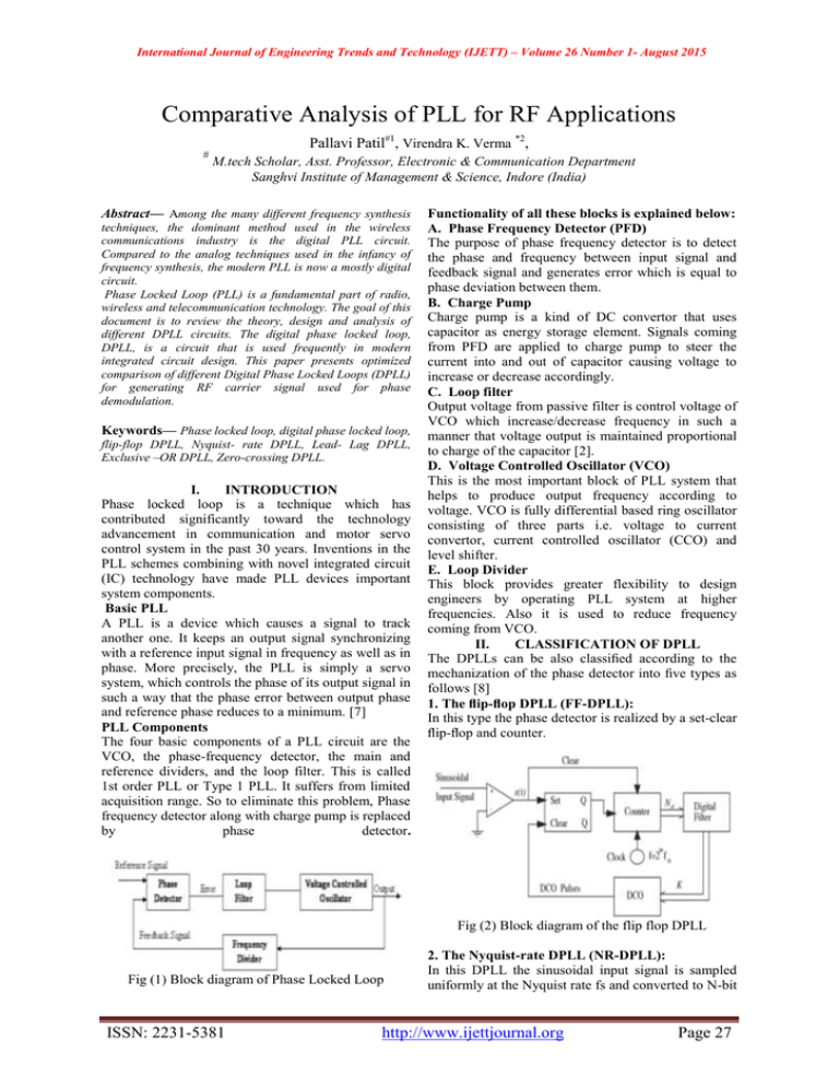
International Journal of Engineering Trends and Technology (IJETT) – Volume 26 Number 1- August 2015 Comparative Analysis of PLL for RF Applications Pallavi Patil#1, Virendra K. Verma *2, # M.tech Scholar, Asst. Professor, Electronic & Communication Department Sanghvi Institute of Management & Science, Indore (India) Abstract— Among the many different frequency synthesis techniques, the dominant method used in the wireless communications industry is the digital PLL circuit. Compared to the analog techniques used in the infancy of frequency synthesis, the modern PLL is now a mostly digital circuit. Phase Locked Loop (PLL) is a fundamental part of radio, wireless and telecommunication technology. The goal of this document is to review the theory, design and analysis of different DPLL circuits. The digital phase locked loop, DPLL, is a circuit that is used frequently in modern integrated circuit design. This paper presents optimized comparison of different Digital Phase Locked Loops (DPLL) for generating RF carrier signal used for phase demodulation. Keywords— Phase locked loop, digital phase locked loop, flip-flop DPLL, Nyquist- rate DPLL, Lead- Lag DPLL, Exclusive –OR DPLL, Zero-crossing DPLL. I. INTRODUCTION Phase locked loop is a technique which has contributed significantly toward the technology advancement in communication and motor servo control system in the past 30 years. Inventions in the PLL schemes combining with novel integrated circuit (IC) technology have made PLL devices important system components. Basic PLL A PLL is a device which causes a signal to track another one. It keeps an output signal synchronizing with a reference input signal in frequency as well as in phase. More precisely, the PLL is simply a servo system, which controls the phase of its output signal in such a way that the phase error between output phase and reference phase reduces to a minimum. [7] PLL Components The four basic components of a PLL circuit are the VCO, the phase-frequency detector, the main and reference dividers, and the loop filter. This is called 1st order PLL or Type 1 PLL. It suffers from limited acquisition range. So to eliminate this problem, Phase frequency detector along with charge pump is replaced by phase detector. Functionality of all these blocks is explained below: A. Phase Frequency Detector (PFD) The purpose of phase frequency detector is to detect the phase and frequency between input signal and feedback signal and generates error which is equal to phase deviation between them. B. Charge Pump Charge pump is a kind of DC convertor that uses capacitor as energy storage element. Signals coming from PFD are applied to charge pump to steer the current into and out of capacitor causing voltage to increase or decrease accordingly. C. Loop filter Output voltage from passive filter is control voltage of VCO which increase/decrease frequency in such a manner that voltage output is maintained proportional to charge of the capacitor [2]. D. Voltage Controlled Oscillator (VCO) This is the most important block of PLL system that helps to produce output frequency according to voltage. VCO is fully differential based ring oscillator consisting of three parts i.e. voltage to current convertor, current controlled oscillator (CCO) and level shifter. E. Loop Divider This block provides greater flexibility to design engineers by operating PLL system at higher frequencies. Also it is used to reduce frequency coming from VCO. II. CLASSIFICATION OF DPLL The DPLLs can be also classified according to the mechanization of the phase detector into five types as follows [8] 1. The flip-flop DPLL (FF-DPLL): In this type the phase detector is realized by a set-clear flip-flop and counter. Fig (2) Block diagram of the flip flop DPLL Fig (1) Block diagram of Phase Locked Loop ISSN: 2231-5381 2. The Nyquist-rate DPLL (NR-DPLL): In this DPLL the sinusoidal input signal is sampled uniformly at the Nyquist rate fs and converted to N-bit http://www.ijettjournal.org Page 27 International Journal of Engineering Trends and Technology (IJETT) – Volume 26 Number 1- August 2015 digital signal by an analog-to-digital converter (ADC), and then it is multiplied digitally by the DCO output v (k) to form an error signal. This error signal is applied to N-bit digital filter whose output controls the period of the DCO. 5. Zero-crossing DPLL (ZC-DPLL): This type of DPLLs accepts sinusoidal signals and samples the input signal at or near zero crossings, hence the name zero-crossing DPLL (ZC-DPLL). There are two variations of ZC-DPLLs. The first, named ZC1−DPLL, samples only on the positivegoing zero crossings, while the other type, ZC2 −DPLL, samples on both positive and negative-going zero crossings. Fig (3) Block diagram of the Nyquist-rate DPLL 3. The lead-lag DPLL (LL-DPLL), a.k.a binaryquantized DPLL (BQ-DPLL): The LL-DPLL is characterized by the binary output of the phase detector that indicates whether the DCO waveform leads or lags the input signal. Due to this quantization it is often named “binary quantized DPLL”. The input sinusoidal signal should be converted to a square wave by a comparator. On the occurrence of a DCO pulse, either “lead” or “lag” terminal of the phase detector will give a pulse depending on the state of the input signal being “high” or “low”, respectively. These pulses are applied to a special type of digital filters known as “sequential filter.” The sequential filter deals with the input “lead” and “lag” pulses statistically; it observes them for a variable duration of time and gives a decision when a reliable limit is reached. Fig (4) Block diagram of the lead-lag DPLL 4. Exclusive-OR DPLL (XOR-DPLL): Greer has utilized an exclusive-OR gate as a phase detector. He used a K-counter as a digital filter and an increment-decrement (I/D) counter with a divide-by-N counter as a DCO. Fig (5) block diagram of the Exclusive-OR DPLL ISSN: 2231-5381 Fig (6) Block diagram of Zero-crossing DPLL (ZC1DPLL) III. TABLE (1) Comparative analysis of different types of DPLLS Flip-flop DPLL(FFD PLL) Nyquistrate DPLL (NRDPLL) Lead-lag DPLL (LLDPLL) BLOCK S USED Phase detector, loop filter,digital control ADC, loop filter,algo rithimic DCO Phase detector, loop filter, divide counter PHASE DETEC TOR (PD) USED LOOP FILTER Flipflop counter type Analog to digital convertor Phase frequenc y detector Digital filter Sequentia l filter K counter ADVAN TAGE N bit outputs are possible. N- bit digital filter It has simple structure. It perfectly works as an integrator . DISAD VANTA GE Circuit is not simple. It requires three frequency inputs. It is easily adapted to operate in conjuncti on with an XOR phase detector. It does not perfectly work as an integrator . DPLLS (PARA METER S) It does not offer jitter design criterion. http://www.ijettjournal.org Exclusive -OR DPLL (XORDPLL) Phase detector,f ilter,I/D counter with divide by N counter as DCO Exclusive OR gate type It does not operate with other detectors except XOR or JK FF. Page 28 Zerocrossin g DPLL (ZCDPL ADC, loop filter DCO Phase detecto r N- bit digital filter Good control over hold range and lock in range. It is not suitabl e for softwar e implem entatio ns. International Journal of Engineering Trends and Technology (IJETT) – Volume 26 Number 1- August 2015 Apart from the classification of different DPLLs there are various other circuits of DPLL which are different from one another in different sections. I have given my best to put a brief comparative analysis among the different DPLLs circuits described in the papers. IV. TABLE (2) Performance comparison of different DPLLs used in various papers PARAMETERS [1] TECHNOLOGY 0.45um [2] [4] 0.25 um 0.35 um 1P3 M CM OS 900 (uW/ MHz ) @210MHz @500 MHz 25 mW 1.2V 3.3V 1.9V 3.3V 6.54-105MHz 45-510 MHz 8.5660 MHz 300 MHz POWER DISSIPATION SUPPLY VOLTAGE FREQUENCY V. [3] APPLICATIONS of PLLS Phase-locked loops are widely used for synchronization purposes: In space communications for coherent demodulation and threshold extension. Phase locked loop can also be used to demodulate the frequency modulated signals. external VI. connections, while maintaining precise timing relationships. ADVANTAGES OF DIGITAL PHASE LOCKED LOOP Digital PLLs (DPLLs) are attracting more attention for the significant advantages of digital systems over their analog counterparts. These advantages include superiority in performance; speed, reliability, and reduction in size and cost.DPLLs do not suffer from the sensitivity of the voltage-controlled oscillator (which decides the center frequency) to temperature and power supply variations, hence the need for initial calibration and periodic adjustment. DPLLs can operate at very low frequencies that create problems in APLLs. VII. CONCLUSION This paper serves as an introduction for this DPLL special section. It provides a concise review of the basic DPLL principles applicable to communication and servo control system gives the configuration of DPLL applications and reports a number of popular DPLL chips. This paper has only talked about the comparison of different digital phase locked loop circuits. The implementation of these circuits will be done in the future work. There are many improvements and concepts that still need to be learned, but the basics of all DPLLs implementation are covered during this project. ACKNOWLEDGEMENT I have taken efforts to make this study. As with any enterprise, this research work could not have been completed without help and support of others. I would like to thanks my research advisor Mr. Virendra Verma for his valuable contributions. In radio transmitters, a PLL is used to REFERENCES synthesize new frequencies which are a multiple of a reference frequency, with the [1] same stability as the reference frequency. Demodulation of AM and FM signals. Recovery of small signals that otherwise [2] would be lost in noise (lock in amplifiers to [3] track the reference frequency) Recovery of clock timing information from a [4] data stream such as from disk drives. Clockmultipliers in microprocessors that allow internal processor elements to run faster than ISSN: 2231-5381 [5] DESIGN OF ALL DIGITAL PHASE LOCKED LOOP (D-PLL) WITH FAST ACQUISITION TIME , M. Bharath Reddy 1, M. Sai Sarath Kumar 2, B. Suresh Kumar 3 1 IJRET: International Journal of Research in Engineering and Technology , eISSN: 2319-1163 | pISSN: 2321-7308 H.-T.Ahm and D.J.Allstot,”A low-jitter 1.9-V CMOS PLL for ultraSPARC microprocessor applications,”IEEE J.Solid-States Circuits, vol.35,pp.450-454,May 1999. ] I.Hwang, S.Lee, S.Lee and S.Kim,”A digitally controlled phase locked loop with fast locking scheme for clock synthesis applications,”in IEEE Int.Solid-State circuits Conf.Dig.Tech.Papers, Feb.2000, pp.168-169. A 300MHz Direct Digital Frequency Synthesizer Based on Improved Redundant prediction CORDIC in 0.35um CMOS Pei-Lin Liu1*, Yi-Ding Huang2, Yue Huang3,Shu-Qin Wan4,78-1-4244-5798-4/10/$26.00 ©2010 IEEE Design of a PLL Based Frequency Synthesizer for WiMAX Applications Mohsen Tamaddon, Milad Ataei, http://www.ijettjournal.org Page 29 International Journal of Engineering Trends and Technology (IJETT) – Volume 26 Number 1- August 2015 [6] [7] [8] [9] [10] [11] [12] [13] [14] [15] [16] [17] and Abdolreza Nabavi Proceedings of ICEE 2010, May 1113, 2010 978-1-4244-6760-0/10/$26.00 ©2010 IEEE Al- Araji, S.R. Hussain, Z.M.;Al- Qutayri, M.A. “Digital Phase Lock Loops, Architecture and Applications” 2006, ,192p., Hardcover ISBN: 978-0-387-32863-8. Kanika Garg “DeSIGN OF LOW POWER PHASE LOCKED LOOP IN SUBMICRON TECHNOLOGY” International Journal of Advanced Technology & Engineering Research (IJATER) ,ISSN NO: 2250-3536 , VOLUME 2, ISSUE 2, MARCH 2012 M. Bharath Reddy 1, M. Sai Sarath Kumar 2, B. Suresh Kumar 3 “Design of all digital phase locked loop (D-PLL) with fast acquisition time” IJRET: International Journal of Research in Engineering and Technology ISSN: 2319-1163 pISSN: 2321-7308 Abishek Mann “The Design of a Low-Power LowNoise Phase Lock Loop”, IEEE Proceedings of ISQED.2010.5450522, April 2010. Feng Lin “Research and Design of Low Jitter, Wide Locking-Range All-Digital Phase-Locked and DelayLocked Loops” PhD Thesis, Electrical Engineering, March 2000. Kanika Garg “DeSIGN OF LOW POWER PHASE LOCKED LOOP IN SUBMICRON TECHNOLOGY” International Journal of Advanced Technology & Engineering Research (IJATER) ,ISSN NO: 2250 , VOLUME 2, ISSUE 2, MARCH 2012 Gayathri M G “Design of All Digital Phase Locked Loop in VHDL” International Journal of Engineering Research and Applications (IJERA) , ISSN: 2248-9622 ,Vol. 3, Issue 4, Jul-Aug 2013, pp.1074-1076 Dr. P.H.Tandel, Anuradha P. Gharge, “Design of General Order Digital Phase Locked Loop” ISSN: 2277-3754 ISO 9001:2008 Certified International Journal of Engineering and Innovative Technology (IJEIT) Volume 2, Issue 7, and January 2013 AbhilashaN.S, “OPTIMIZED DESIGN OF DIGITAL PHASE LOCKED LOOPS FOR RF CARRIER ACQUISITION” [Abhilashaetal,3(5):May,2014] ISSN:2277-9655 ,Scientific Journal Impact Factor: 3.449 (ISRA), Impact Factor: 1.852 R.B. Staszewski,D. Leipold,K. Muhammad, and P. T.Balsara, “Digitally controlled oscillator (DCO)-based architecture for RF frequency synthesis in a deepsubmicrometer CMOS process,” IEEE Trans. Circuits Syst. II., vol. 50, no. 11, pp. 815–828, Nov. 2003. Behavioural Modelling and Simulation of PLL Based Integer N Frequency Synthesizer using Simulink ,Jyoti P. Patra and Umesh C. Pati International Journal of Electronics and Communication Engineering. ISSN 09742166 Volume 5, Number 3 (2012), pp. 351-362 Guan-Chyun Hsieh, Senior Member and James C, Hung, Fellow “Phased- Locked Loop Techniques- A Survey” IEEE Transactions on Industrial Electronics, Vol. 43,No. 6, Dec 1996. ISSN: 2231-5381 http://www.ijettjournal.org Page 30
