HMC625BLP5E T 0.5 dB LSB GaAs MMIC 6-BIT DIGITAL
advertisement

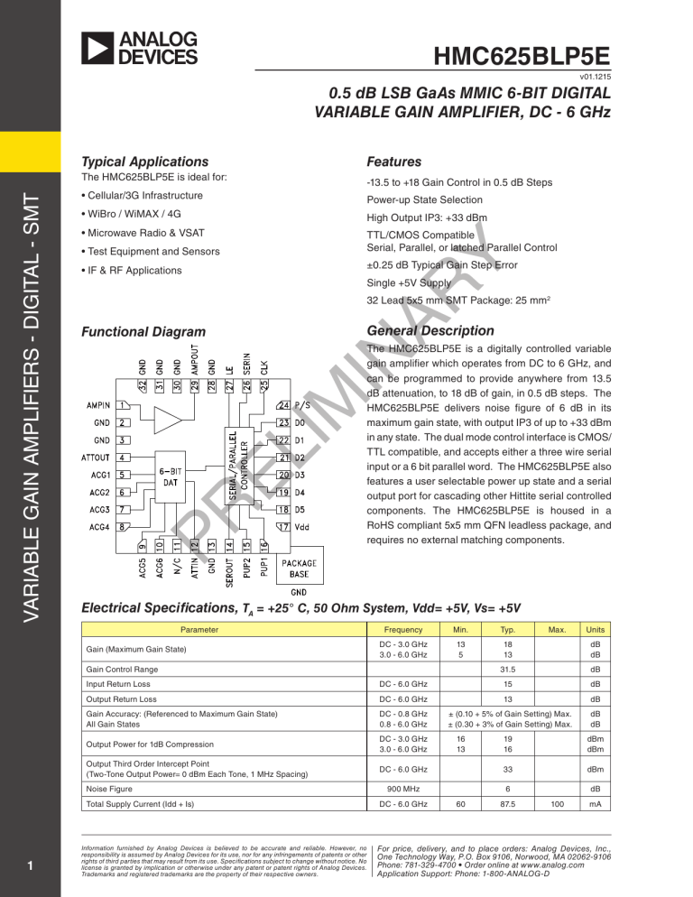
HMC625BLP5E v01.1215 0.5 dB LSB GaAs MMIC 6-BIT DIGITAL VARIABLE GAIN AMPLIFIER, DC - 6 GHz Typical Applications Features -13.5 to +18 Gain Control in 0.5 dB Steps • Cellular/3G Infrastructure Power-up State Selection • WiBro / WiMAX / 4G High Output IP3: +33 dBm • Microwave Radio & VSAT • Test Equipment and Sensors TTL/CMOS Compatible Serial, Parallel, or latched Parallel Control • IF & RF Applications ±0.25 dB Typical Gain Step Error PR EL IM IN AR Y VARIABLE GAIN AMPLIFIERS - DIGITAL - SMT The HMC625BLP5E is ideal for: Single +5V Supply 32 Lead 5x5 mm SMT Package: 25 mm2 Functional Diagram General Description The HMC625BLP5E is a digitally controlled variable gain amplifier which operates from DC to 6 GHz, and can be programmed to provide anywhere from 13.5 dB attenuation, to 18 dB of gain, in 0.5 dB steps. The HMC625BLP5E delivers noise figure of 6 dB in its maximum gain state, with output IP3 of up to +33 dBm in any state. The dual mode control interface is CMOS/ TTL compatible, and accepts either a three wire serial input or a 6 bit parallel word. The HMC625BLP5E also features a user selectable power up state and a serial output port for cascading other Hittite serial controlled components. The HMC625BLP5E is housed in a RoHS compliant 5x5 mm QFN leadless package, and requires no external matching components. Electrical Specifications, TA = +25° C, 50 Ohm System, Vdd= +5V, Vs= +5V Parameter Gain (Maximum Gain State) Frequency Min. Typ. DC - 3.0 GHz 3.0 - 6.0 GHz 13 5 18 13 dB dB 31.5 dB 15 dB Gain Control Range Input Return Loss Units Output Return Loss DC - 6.0 GHz 13 dB Gain Accuracy: (Referenced to Maximum Gain State) All Gain States DC - 0.8 GHz 0.8 - 6.0 GHz ± (0.10 + 5% of Gain Setting) Max. ± (0.30 + 3% of Gain Setting) Max. dB dB Output Power for 1dB Compression DC - 3.0 GHz 3.0 - 6.0 GHz Output Third Order Intercept Point (Two-Tone Output Power= 0 dBm Each Tone, 1 MHz Spacing) Noise Figure Total Supply Current (Idd + Is) 1 DC - 6.0 GHz Max. Information furnished by Analog Devices is believed to be accurate and reliable. However, no responsibility is assumed by Analog Devices for its use, nor for any infringements of patents or other rights of third parties that may result from its use. Specifications subject to change without notice. No license is granted by implication or otherwise under any patent or patent rights of Analog Devices. Trademarks and registered trademarks are the property of their respective owners. 19 16 dBm dBm DC - 6.0 GHz 33 dBm 900 MHz 6 dB DC - 6.0 GHz 16 13 60 87.5 100 mA For price, delivery, and to place orders: Analog Devices, Inc., One Technology Way, P.O. Box 9106, Norwood, MA 02062-9106 Phone: 781-329-4700 • Order online at www.analog.com Application Support: Phone: 1-800-ANALOG-D HMC625BLP5E v01.1215 0.5 dB LSB GaAs MMIC 6-BIT DIGITAL VARIABLE GAIN AMPLIFIER, DC - 6 GHz Outline Drawing Pin Descriptions Function Description 1 AMPIN This pin is DC coupled. An off chip DC blocking capacitor is required. 2, 3, 13, 28, 30 - 32 4, 12 5 - 10 11 14 15, 16 AMPOUT RF output and DC bias (Vcc) for the output stage of the amplifier. GND These pins and package bottom must be connected to RF/DC ground. ATTIN, ATTOUT These pins are DC coupled and matched to 50 Ohms. Blocking capacitors are required. Select value based on lowest frequency of operation. ACG1 - ACG6 External capacitors to ground is required. Select value for lowest frequency of operation. Place capacitor as close to pins as possible. N/C The pins are not connected internally; however, all data shown herein was measured with these pins connected to RF/DC ground externally. SEROUT Serial input data delayed by 6 clock cycles. PR EL IM IN AR Y 29 Interface Schematic PUP2, PUP1 18 - 23 D5, D4, D3, D2, D1, D0 24 P/S 25 CLK 26 SERIN 27 LE 17 Vdd VARIABLE GAIN AMPLIFIERS - DIGITAL - SMT Pin Number Supply Voltage For price, delivery, and to place orders: Analog Devices, Inc., One Technology Way, P.O. Box 9106, Norwood, MA 02062-9106 Phone: 781-329-4700 • Order online at www.analog.com Application Support: Phone: 1-800-ANALOG-D 2 HMC625BLP5E v01.1215 0.5 dB LSB GaAs MMIC 6-BIT DIGITAL VARIABLE GAIN AMPLIFIER, DC - 6 GHz 3 PR EL IM IN AR Y VARIABLE GAIN AMPLIFIERS - DIGITAL - SMT Package Information NOTES: 1. LEADFRAME MATERIAL: COPPER ALLOY 2. DIMENSIONS ARE IN INCHES [MILLIMETERS] 3. LEAD SPACING TOLERANCE IS NON-CUMULATIVE. 4. PAD BURR LENGTH SHALL BE 0.15mm MAXIMUM. PAD BURR HEIGHT SHALL BE 0.05mm MAXIMUM. 5. PACKAGE WARP SHALL NOT EXCEED 0.05mm. 6. ALL GROUND LEADS AND GROUND PADDLE MUST BE SOLDERED TO PCB RF GROUND. 7. REFER TO HITTITE APPLICATION NOTE FOR SUGGESTED LAND PATTERN. Part Number Package Body Material Lead Finish HMC625aLP5E RoHS-compliant Low Stress Injection Molded Plastic 100% matte Sn MSL Rating MSL3 [1] Package Marking [2] H625B XXXX [1] Max peak reflow temperature of 260 °C [2] 4-Digit lot number XXXX For price, delivery, and to place orders: Analog Devices, Inc., One Technology Way, P.O. Box 9106, Norwood, MA 02062-9106 Phone: 781-329-4700 • Order online at www.analog.com Application Support: Phone: 1-800-ANALOG-D


