Differential Driver
Evaluation Board
EVAL-ADDIFFAMP
FEATURES
GENERAL DESCRIPTION
Flexible board layout
Accomodates AD8131/AD8132/AD8138/AD8139
Accomodates various circuit configurations:
4-resistor
Two different feedback loops
Input and output transformers
Filters
An Analog Devices differential driver evaluation board makes it
easy for designers to get quick performance results for their
particular differential driver application circuits. The board
layout is very flexible and allows for many circuit configurations, including traditional 4-resistor circuits, circuits with two
different feedback loops, circuits with input and output
transformers, filters, and many others. Most resistors and
capacitors are in 1206 packages.
The board accommodates the AD8131, AD8132, AD8138, and
AD8139. Use the data sheets for these devices with this
evaluation board data sheet.
The AD8131 is a special case because it has internal feedback
networks but can, nonetheless, be evaluated on the board by:
•
Omitting the R19 and R20 feedback resistors and C3 and
C4 capacitors.
•
Using 0 Ω resistors for Gain Resistor R17 and Gain
Resistor R18.
•
Ignoring all further references to these components.
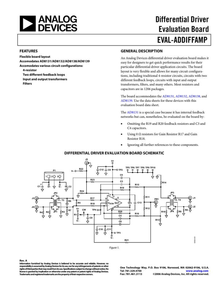
DIFFERENTIAL DRIVER EVALUATION BOARD SCHEMATIC
J5
2
TP5 TP6 TP7 TP8 TP9 TP10
R22
P1
1
V+
C12
V–
C8
TP2
C5
3
R23
+
C1
V+
V–
+
C3
R19
R24
JP2
JP3
7
R17
J3
T1, T3
R6
J4
R4
R2
JP1
R14
R15
C2
R3
R7
R5
V+
TP4
R11
5
8
2
DUT
V
1 OCM
4
6
R20
R18
CW
3
TP1
T2, T4
C13
J2
R12
R10
R16
R1
J1
PR1
JP4
R9
R8
C4
C9
V–
R13
C6
C10
C11
V–
R21
02838-001
TP3
Figure 1.
Rev. A
Information furnished by Analog Devices is believed to be accurate and reliable. However, no
responsibility is assumed by Analog Devices for its use, nor for any infringements of patents or other
rights of third parties that may result from its use. Specifications subject to change without notice. No
license is granted by implication or otherwise under any patent or patent rights of Analog Devices.
Trademarks and registered trademarks are the property of their respective owners.
One Technology Way, P.O. Box 9106, Norwood, MA 02062-9106, U.S.A.
Tel: 781.329.4700
www.analog.com
Fax: 781.461.3113
©2006 Analog Devices, Inc. All rights reserved.
EVAL-ADDIFFAMP
HARDWARE
POWER SUPPLIES
Power is applied to the board through P1, a Molex®
22-11-2032 3-pin header. Pin 1 (square footprint) is for the
positive supply, Pin 3 is for the negative supply, and Pin 2 is
connected to the ground plane of the board. Alternatively,
looped test points can be used; Test Point TP2 connects to the
positive supply, TP3 connects to the negative supply, and TP7
and TP8 connect to the ground plane. The TP5, TP6, TP9, and
TP10 test points also connect to the ground plane.
The board accommodates single or dual supplies. For singlesupply operation, simply connect the negative supply to the
ground plane.
It is very important that the power supply pins of the device
under test (DUT) have broadband decoupling circuitry. The
board layout facilitates this with footprints for two 1206 ceramic
capacitors on each supply. At frequencies beyond the resonant
frequency of the first capacitor and its associated internal and
external inductance, the second capacitor provides the required
low impedance return current path. For optimum performance,
place the smaller of the two capacitances closest to the DUT, in
positions C8 and C11. C13 provides the user with the option of
adding differential decoupling between the supplies. Bulk
decoupling is provided by C1 and C2; 10 μF tantalum capacitors
are recommended.
FEEDBACK NETWORKS AND INPUT/OUTPUT
TERMINATIONS
R19 and R17 compose the upper resistive feedback loop (see
Figure 1), and R20 and R18 compose the lower feedback loop.
C3 and C4 are included across the feedback resistors to provide
frequency-dependent feedback, typically used to introduce a
real-axis pole in the closed-loop frequency response.
To minimize summing node capacitances, void the ground
plane under and around Pin 1 and Pin 8 of the DUT and the
copper that connects to them.
R15 and R16 series termination resistors are provided on each
of the outputs for impedance matching, analog-to-digital
converter (ADC) driving, and other system requirements.
VOCM INPUT
The VOCM input can be set to a dc level by adjusting Potentiometer R1 that spans the power supplies. For the dc case, C9 is
provided at the wiper for decoupling.
An external voltage can be applied to VOCM via TP4 (referenced
to the ground plane of the board). In ADC driving applications,
it is convenient to apply the ADC dc reference voltage output
directly to TP4.
It is also possible to drive the VOCM input from an external ac
source. In this case, omit C9 or reduce it to a value that allows
the desired signal to be passed. For high frequency signals on
VOCM, connect the center conductor of a coaxial cable to TP4
and ground its shield at TP10.
R21 is provided for the high common-mode output impedance
application illustrated in Figure 77 of the AD8132 data sheet.
MEASURING OUTPUT COMMON-MODE VOLTAGE
The internal common-mode feedback loop used in the
differential drivers forces the output common-mode voltage to
be equal to the voltage applied to the VOCM input, thereby
providing excellent output balance. R11 and R12 form a voltage
divider across the differential output, and the voltage at the
divider tap is equal to the output common-mode voltage,
provided R11 and R12 are exactly matched in value. If R11 and
R12 are used to evaluate the output common-mode voltage,
they should be measured and matched to better than 300 ppm
to obtain results commensurate with the DUT output balance
error performance of −70 dB. The Test Point PR1 accepts
coaxial-type oscilloscope test points, such as the Berg
Electronics 33JR135-1.
INPUT/OUTPUT TRANSFORMERS
R6 and R7 are included as input termination resistors for
applications that have single-ended inputs. Having a place for a
shunt resistor on each input makes it simple to match the two
feedback factors. A common example of how this is used is
when the input signal originates from an unbalanced 50 Ω
source. In this case, the single-ended termination resistance is
50 Ω and the Thevenin equivalent resistance seen looking back
to the source is 25 Ω. For the traditional 4-resistor configuration,
where R19 = R20 and R17 = R18, the feedback networks are
matched by making the shunt resistor on the input leg opposite
the termination resistor equal to 25 Ω. R5 is provided for differential termination.
The board has the added flexibility of allowing the user to
incorporate transformers on its input and output. This
capability can be especially useful when connecting to singleended test equipment. Because both input and output
transformers have dual, nested footprints, the user can select
from a wide array of transformers available from companies
such as Mini-Circuits® and Coilcraft®. The layout provides
footprints for connecting resistors to ground on the primary
and secondary transformer center taps, offering the user a
number of options with regard to the common-mode properties
of the evaluation circuit.
JP1, JP2, JP3, and JP4 are jumpers on the backside of the board
that provide direct shunts across their associated transformers.
Rev. A | Page 2 of 4
EVAL-ADDIFFAMP
When not using a transformer, bypassing the transformer is a
simple matter of shorting the appropriate jumpers. Clearly,
when using a transformer, it is a good idea to verify that the
associated jumpers are open.
user to be more creative than the traditional designs. Clearly, a
component labeled as a capacitor need not be a capacitor
provided it fits the user’s application circuit and to the footprint
on the board.
SMA INPUT/OUTPUT CONNECTORS
In application circuits where footprints for desired components
are not available on the board, the user is encouraged to find ways
to include them. For example, if an additional shunt element
were required, the user could scrape some solder mask away
from the ground plane and trace (if necessary) to make a place
for the additional part. Furthermore, 1206 elements can be
stacked on top of each other to implement a parallel circuit. An
example of this would be stacking capacitors across R17 and
R18 to realize a zero in the closed-loop transfer function. This is
one way to insert pre-emphasis in a line-driver application.
The inputs and outputs have edge-mounted SMA connectors
for straightforward connection to coaxial cables. The recommended connector type is Johnson Components™ part number
142-0701-801, or equivalent.
OTHER COMPONENTS
The components discussed in this data sheet pertain mostly to
traditional amplifier topologies. There are footprints provided
for a number of other components on the board to allow the
Rev. A | Page 3 of 4
EVAL-ADDIFFAMP
ORDERING INFORMATION
ORDERING GUIDE
Model
EVAL-ADDIFFAMP-1R
EVAL-ADDIFFAMP-1RM
Description
Differential Driver Evaluation Board (SOIC)
Differential Driver Evaluation Board (MSOP)
ESD CAUTION
ESD (electrostatic discharge) sensitive device. Electrostatic charges as high as 4000 V readily accumulate on
the human body and test equipment and can discharge without detection. Although this product features
proprietary ESD protection circuitry, permanent damage may occur on devices subjected to high energy
electrostatic discharges. Therefore, proper ESD precautions are recommended to avoid performance
degradation or loss of functionality.
REVISION HISTORY
1/06—Rev. 0 to Rev. A
Updated Format..................................................................Universal
Change to Figure 1 ........................................................................... 1
10/03—Revision 0: Initial Version
©2006 Analog Devices, Inc. All rights reserved. Trademarks and
registered trademarks are the property of their respective owners.
EB04519-0-1/06(A)
T
T
Rev. A | Page 4 of 4
