An Inside Look at High Speed Analog-to-Digital Converter Accuracy |
advertisement
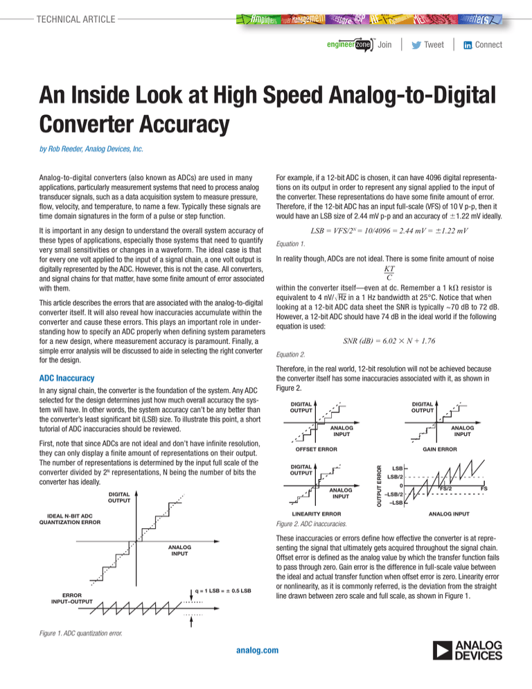
TECHNICAL ARTICLE | Join | Tweet Connect An Inside Look at High Speed Analog-to-Digital Converter Accuracy by Rob Reeder, Analog Devices, Inc. Analog-to-digital converters (also known as ADCs) are used in many applications, particularly measurement systems that need to process analog transducer signals, such as a data acquisition system to measure pressure, flow, velocity, and temperature, to name a few. Typically these signals are time domain signatures in the form of a pulse or step function. For example, if a 12-bit ADC is chosen, it can have 4096 digital representations on its output in order to represent any signal applied to the input of the converter. These representations do have some finite amount of error. Therefore, if the 12-bit ADC has an input full-scale (VFS) of 10 V p-p, then it would have an LSB size of 2.44 mV p-p and an accuracy of ±1.22 mV ideally. It is important in any design to understand the overall system accuracy of these types of applications, especially those systems that need to quantify very small sensitivities or changes in a waveform. The ideal case is that for every one volt applied to the input of a signal chain, a one volt output is digitally represented by the ADC. However, this is not the case. All converters, and signal chains for that matter, have some finite amount of error associated with them. LSB = VFS/2N = 10/4096 = 2.44 mV = ±1.22 mV ADC Inaccuracy In any signal chain, the converter is the foundation of the system. Any ADC selected for the design determines just how much overall accuracy the system will have. In other words, the system accuracy can’t be any better than the converter’s least significant bit (LSB) size. To illustrate this point, a short tutorial of ADC inaccuracies should be reviewed. In reality though, ADCs are not ideal. There is some finite amount of noise KT C within the converter itself—even at dc. Remember a 1 kΩ resistor is equivalent to 4 nV/∙ Hz in a 1 Hz bandwidth at 25°C. Notice that when looking at a 12-bit ADC data sheet the SNR is typically ~70 dB to 72 dB. However, a 12-bit ADC should have 74 dB in the ideal world if the following equation is used: SNR (dB) = 6.02 × N + 1.76 Equation 2. Therefore, in the real world, 12-bit resolution will not be achieved because the converter itself has some inaccuracies associated with it, as shown in Figure 2. DIGITAL OUTPUT ANALOG INPUT First, note that since ADCs are not ideal and don’t have infinite resolution, they can only display a finite amount of representations on their output. The number of representations is determined by the input full scale of the converter divided by 2N representations, N being the number of bits the converter has ideally. DIGITAL OUTPUT ANALOG INPUT LINEARITY ERROR IDEAL N-BIT ADC QUANTIZATION ERROR ANALOG INPUT OFFSET ERROR DIGITAL OUTPUT GAIN ERROR LSB LSB/2 0 –LSB/2 FS/2 FS –LSB ANALOG INPUT Figure 2. ADC inaccuracies. ANALOG INPUT ERROR INPUT–OUTPUT DIGITAL OUTPUT OUTPUT ERROR This article describes the errors that are associated with the analog-to-digital converter itself. It will also reveal how inaccuracies accumulate within the converter and cause these errors. This plays an important role in understanding how to specify an ADC properly when defining system parameters for a new design, where measurement accuracy is paramount. Finally, a simple error analysis will be discussed to aide in selecting the right converter for the design. Equation 1. q = 1 LSB = ± 0.5 LSB These inaccuracies or errors define how effective the converter is at representing the signal that ultimately gets acquired throughout the signal chain. Offset error is defined as the analog value by which the transfer function fails to pass through zero. Gain error is the difference in full-scale value between the ideal and actual transfer function when offset error is zero. Linearity error or nonlinearity, as it is commonly referred, is the deviation from the straight line drawn between zero scale and full scale, as shown in Figure 1. Figure 1. ADC quantization error. analog.com More on ADC Inaccuracies Now that the most basic analog-to-digital converter errors have been defined and understood, it is useful to describe the differences between these errors. Typically, most ADCs have such small offset and gain errors associated with them that they can either be ignored or adjusted (nulled) via an external analog circuit, or corrected digitally. However, other errors like linearity, quantization, and tempco cannot be easily adjusted or eliminated. Analog-to-digital converter linearity is only as good as the converter itself, which depends on architecture and process variation. There are ways to correct for this but they are expensive. The designer has two choices, either purchase a better, more expensive converter, or digitally correct the linearity. Digital correction can be expensive too. This means more resource requirements may be involved in specifying a DSP or FPGA because linearity will shift over temperature and process variation. Depending on the sample rate, IF, and resolution, digital correction can require extensive characterization and lookup tables in order to correct or adjust the ADC’s performance on-the-fly. Linearity has two types of errors: they are differential nonlinearity and integral linearity, commonly referred to as DNL and INL, respectively. DNL is defined as any error or deviation from its ideal value. In other words, it is the deviation in the analog difference between two adjacent codes, from the ideal code value of VFS/2N. Think of this in relation to SNR performance of the ADC. As the code variation gets bigger, the number of transitions decreases. This error is bound to ±0.5 LSBs over temperature to ensure no missing codes. INL is defined as the curvature deviation from the ideal straight line approximation between zero and full scale. INL, for the most part, determines the SFDR performance of the ADC. The shape of the overall INL deviation can determine the dominant harmonic performance. For instance, a bow in the INL curve will consistently yield worse even order harmonics and an s-bow in the INL curve will commonly yield odd order harmonics. This error is frequency dependent in nature and doesn’t relate to this type of error analysis. Even though a null in the static offset and gain errors is feasible, temperature coefficients related to offsets and gain errors will still exist. For example, a 12-bit ADC with 10 ppm gain error or FSR/°C = 0.001%/°C. • Power supply sensitivity, which is typically in the form of low frequency PSRR (power supply rejection ratio) within the first Nyquist zone. This can be typically expressed as 60 dB or ±2 LSBs for a 12-bit ADC. By simply taking the root-sum-square (RSS), all these error sources = ±3.5 LSBs of total converter error. This might seem overly pessimistic. Yet a statistical tolerance may be overly optimistic, or the total sum of errors divided by the number of errors, or (0.5 + 2.5 + 1.3 + 2)/4 = ±1.58 LSBs. Finding the actual tolerance of the ADC should be somewhere between these two thoughts or methods. Therefore, when adding accuracy errors in the converter, or any accuracy system analysis, the designer should use a weighted error source approach, then RSS these error sources together. This will provide the best method in determining the ADC’s overall error. Therefore, the relative accuracy of ±0.5 LSBs should stay at 100%. However, the gain tempco error of ±2.5 LSBs should be 66% of the total error or 2.5/(0.5 + 1.3 + 2) × 100. The offset tempco error of ±1.3 LSBs would be 26% of the total error or 1.3/(0.5 + 2.5 + 2) × 100. The power supply sensitivity error of ±2 LSBs would be 47% of the total error or 2/(0.5 + 1.3 + 2.5) × 100. Adding these weighted errors together in an RSS fashion or square root ∙((0.5 × 1)2 + (2.5 × 0.66)2 + (1.3 × 0.26)2 + (2 × 0.47)2), provides a total error of ±2.0 LSBs, which yields something more realistic, and in between, the optimistic and pessimistic method outcomes above. Accuracy in ADC Bandwidth The ADC also has a settling time accuracy as well. Keep in mind that a converter’s internal front end needs to have enough bandwidth (BW) in order to accurately sample the signal. Otherwise, an accumulation of errors will be greater than what was discovered above. In general, an ADC’s internal front end needs to settle within a half a period or sample clock cycle (0.5/Fs) in order to provide an inbound accurate representation of the analog signal to be acquired. Therefore, for a 12-bit ADC sampling at 2.5 GSPS and full-scale input range of 1.3 V p-p the full power bandwidth (FPBW) required can be derived starting with the following transient equation: 1 LSB = VFS × e (-t/τ) A 1 LSB in a 12-bit system = 1 part in 4096, or approximately 0.024%. So with a 125°C ∆ (–40°C to +85°C), this yields a ±2.5 LSB gain tempco error or 0.001% × 125 = 0.125%. Solving for t: In which 0.125/0.024 = 5.1 or ±2.55 LSBs. Sub in τ = 1/(2 × π × FPBW), one time constant, and solve for FPBW: For offset tempco a 5 ppm offset error or FSR/°C = 0.0005%/°C. t = −τ × ln(1 LSB/VFS) FPBW = −(1/(2 × π × t)) × ln(1 LSB/VFS) This would yield a ±1.3 LSB offset tempco error or 0.0005% × 125 = 0.0625. In which 0.0625/0.024 = 2.6 or ±1.3 LSBs. Now, let t = 0.5/Fs, the time needed for a sample to settle, where the sampling period is 1/Fs: ADC Error Analysis FPBW = −(Fs/π × ln(1 LSB/VFS) = –(2.5G/π) × ln(317 mV p-p/1.3)) = 6.62 GHz. Other error sources that can also play a role in the converter’s performance are CMRR, clock jitter, and inherent board noise, and coupling, to name a few. All of these errors ultimately define how effective the ADC is at representing a signal, and usually present themselves more effectively in the frequency domain. From a time domain standpoint, the following five errors are needed to dictate the converter’s overall accuracy: • Relative accuracy, DNL, which was defined as ±0.5 LSBs • Relative accuracy tempco and DNL tempco, which is typically included in the relative accuracy specification in the data sheet. • Gain tempco error, which was ±2.5 LSBs (from the previous example) • Offset tempco error, which was ±1.3 LSBs (from the previous example) | An Inside Look at High Speed Analog-to-Digital Converter Accuracy 2 This will yield the minimum required bandwidth for the ADCs internal front end or FPBW. This the amount of BW required for the converter’s internal front end to settle within 1 LSB and sample the analog signal appropriately. This will take several time constants to pass in order to meet an accuracy of 1 LSB for this type of ADC. Where one time constant is equal to 24 ps or τ = 1/(2 × π × FPBW). To understand the number of time constants required for the full-scale range of the ADC in LSB size % full-scale error, or %FS, needs to be found. Or 1 LSB = FS/(2N), where N = number of bits or 1.3 V p-p/(212) = 317 mV p-p, and %FS = (LSB/FS) × 100 = 0.0244. By plotting of Euler’s number, or eτ, a graph can be developed that makes it easy to show the relative error as each time constant passes. As shown in Figure 3 it can be found that it takes 8.4 time constants for the 12-bit ADC example to settle appropriately within 1 LSB. NUMBER OF TIME CONSTANT ANALOG-TO-DIGITAL CONVERTERS NEEDS TO SETTLE ACCURATELY WITHIN ½ LSB 40.00 35.00 30.00 ERROR (%) 25.00 20.00 15.00 6B 10.00 8B 10B 12B 14B 16B 5.00 0.00 0 1 2 3 4 5 6 7 8 9 10 11 12 13 14 15 16 TIME CONSTANT (t) Figure 3: Settling accuracy vs. time constants. This allows the designer to estimate the maximum analog input frequency, or sample BW, that can be used by the converter and still settle within 1 LSB of error. Beyond that, the ADC cannot accurately represent the signal. This is simply defined as FMAX = 1/(τ × number of time constants) or 1/(24 ps × 8.4) = 4.96 GHz. Keep in mind, this represents a best case scenario here and the assumption is for a single-pole model ADC front end. Not all practical converters behave this way, but this is good starting point. For example, the model described is valid up to 12 bits, however, 14-/16-bits and beyond, a second order model should be used based on these subtle effects that can make settling time stretch out beyond the predicted first order models. Quick Note on ADC Bandwidth Keep in mind that an ADC’s full power bandwidth is different from converter usable or sample bandwidth as defined above. This can be thought of as analogous to the full power bandwidth (FPBW) of an op amp, where the signal looks more like a triangle and there is a lot of distortion on its output(s). FPBW is the bandwidth that the ADC needs to acquire signals accurately and for the internal front end to settle properly, (6.62 GHz as shown in the previous example). Selecting an IF and using the converter out in this region is not a good idea, as performance results will widely vary in the system, based on the rated resolution and performance stated in the converter’s data sheet, the full power bandwidth is much bigger than the maximum sample bandwidth of the converter itself, as in ~5 GHz, the example shown above. Sample bandwidth is where the design is centered. All designs should avoid using some or all of the highest frequency portions of the rated full power bandwidth, by doing so expect a derating in dynamic performance (SNR/ SFDR) that could vary widely. To determine the sample bandwidth of the high speed ADC, use the example as shown above, as sometimes this isn’t specially given in the data sheet. Typically, the data sheet has specified or even listed production tested frequencies that guarantee delivered performance within the converter’s sample bandwidth. However, in older ADC generations these test frequencies are not always shown out to the FMAX as defined above in the data sheet. Moving forward, better explanations about these bandwidth terms in the industry need to be specified, defined, and tested. Conclusion This article should have provided some guidance on how to look at general static ADC inaccuracy errors and ADC inaccuracy error that involves bandwidth. A greater understanding of ADC errors and how these errors influence the signal chain has also been given. Keep in mind, that not all components are created equal, and this is true for both active and passive devices. Developing spreadsheets that capture all these errors is an easy way to plug in different signal chain components to make evaluations and component trade-offs more quickly. This is especially true when trading off costs, size, and power between components and signal chain performance differences. Keep these principles in mind when doing the next signal chain design. By request, a spreadsheet analysis can be sent to you highlighting the previously mentioned examples. Feel free to use this and tailor it to your next design. If you have further questions, connect with me on the Analog Devices EngineerZone®, an online technical support community, at RReeder. Further discussions on how to generate a full signal chain analysis will be covered in Part 2: Analog Signal Chain Accuracy. Finally, remember that simply increasing the performance or resolution of the ADC in the signal chain will not increase the measurement accuracy. If the same amount of front-end noise is still present, the accuracy will not improve. The noise will only be measured to a more granular degree and probably cost the designer’s boss more money in the end. References AN010 Application Note, Measurement Dynamic Range for Signal Analyzers. LDS Dactron, 2003. Bennett, William R. “Spectra of Quantized Signals.” Bell System Technical Journal, Vol. 27, 1948. Bennett, William R. “Noise in PCM Systems.” Bell Labs Record, Vol. 26, 1948. Brannon, Brad. AN-410 Application Note, Overcoming Converter Nonlinearities with Dither. Analog Devices, 1995. Gyorki, John R. Signal Conditioning & PC-Based Data Acquisition Handbook. 3rd Edition, 1-11. Kester, Walt. “Analog-Digital Conversion: Seminar Series.” Analog-Digital Conversion, Analog Devices, 2004. Overall Accuracy = ENOB (Effective Number of Bits), Data Translation. Ruscak, Steve and Larry Singer. Using Histogram Techniques to Measure A/D Converter Noise. Analog Dialogue, Vol. 29-2, 1995. “System Error Budgets, Accuracy, Resolution.” Dataforth. Titus, John. “Resolution and Accuracy: Cousins, Not Twins.” Design News, 2003. Online Support Community Engage with the Analog Devices technology experts in our online support community. Ask your tough design questions, browse FAQs, or join a conversation. ez.analog.com analog.com | 3 Analog Devices, Inc. Worldwide Headquarters Analog Devices, Inc. One Technology Way P.O. Box 9106 Norwood, MA 02062-9106 U.S.A. Tel: 781.329.4700 (800.262.5643, U.S.A. only) Fax: 781.461.3113 Analog Devices, Inc. Europe Headquarters Analog Devices, Inc. Wilhelm-Wagenfeld-Str. 6 80807 Munich Germany Tel: 49.89.76903.0 Fax: 49.89.76903.157 Analog Devices, Inc. Japan Headquarters Analog Devices, KK New Pier Takeshiba South Tower Building 1-16-1 Kaigan, Minato-ku, Tokyo, 105-6891 Japan Tel: 813.5402.8200 Fax: 813.5402.1064 Analog Devices, Inc. Asia Pacific Headquarters Analog Devices 5F, Sandhill Plaza 2290 Zuchongzhi Road Zhangjiang Hi-Tech Park Pudong New District Shanghai, China 201203 Tel: 86.21.2320.8000 Fax: 86.21.2320.8222 ©2015 Analog Devices, Inc. All rights reserved. Trademarks and registered trademarks are the property of their respective owners. TA13120-0-4/15 analog.com
