HMC7054 s PA H
advertisement
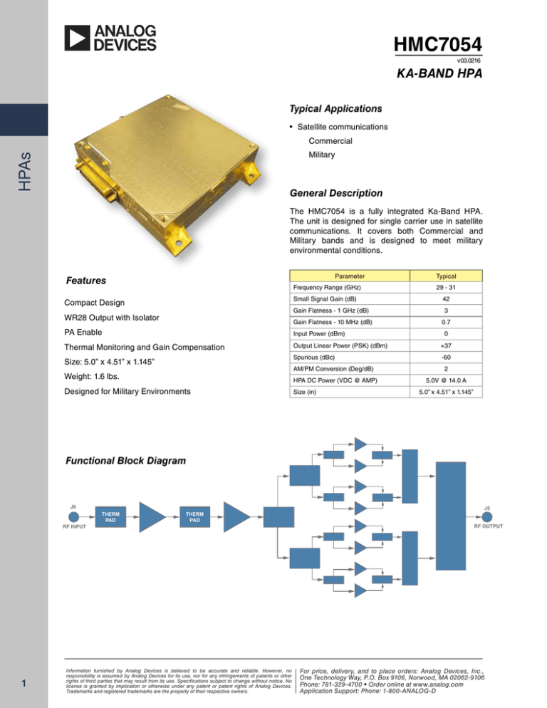
HMC7054 v03.0216 Ka-Band HPA Typical Applications HPAs • Satellite communications Commercial Military General Description The HMC7054 is a fully integrated Ka-Band HPA. The unit is designed for single carrier use in satellite communications. It covers both Commercial and Military bands and is designed to meet military environmental conditions. Parameter Features Frequency Range (GHz) Small Signal Gain (dB) Compact Design WR28 Output with Isolator Typical 29 - 31 42 Gain Flatness - 1 GHz (dB) 3 Gain Flatness - 10 MHz (dB) 0.7 PA Enable Input Power (dBm) Thermal Monitoring and Gain Compensation Output Linear Power (PSK) (dBm) +37 Spurious (dBc) -60 Size: 5.0” x 4.51” x 1.145” AM/PM Conversion (Deg/dB) Weight: 1.6 lbs. HPA DC Power (VDC @ AMP) Designed for Military Environments Size (in) 0 2 5.0V @ 14.0 A 5.0” x 4.51” x 1.145” Functional Block Diagram J9 RF INPUT 1 THERM PAD THERM PAD Information furnished by Analog Devices is believed to be accurate and reliable. However, no responsibility is assumed by Analog Devices for its use, nor for any infringements of patents or other rights of third parties that may result from its use. Specifications subject to change without notice. No license is granted by implication or otherwise under any patent or patent rights of Analog Devices. Trademarks and registered trademarks are the property of their respective owners. J5 RF OUTPUT For price, delivery, and to place orders: Analog Devices, Inc., One Technology Way, P.O. Box 9106, Norwood, MA 02062-9106 Phone: 781-329-4700 • Order online at www.analog.com Application Support: Phone: 1-800-ANALOG-D HMC7054 v03.0216 Ka-Band HPA Electrical Specifications Specification HPAs Parameter Min. Typ. Units Notes Frequency range (MIL) 30 31 GHz Military band Frequency range (COMM) 29 30 GHz Commercial band 5 dBm 5 dBm 42 dB 3 dB Gain flatness -40Mhz 0.7 dB Gain variation (over temp) ±1.0 dB Gain stability ±0.25 dB/24h Group delay - 40MHz ±0.25 nSec Group delay - 10MHz ±0.1 nSec Reference frequency Reference output power 10 -7.5 Input Power Small Signal gain 42 Gain flatness -1Ghz Input (VSWR) MHz 2:1 RF output (VSWR) 1.5:1 Linear power With external Isolator 37 dBm P1dB 38.5 dBm TX maximum power (Psat) 39.5 dBm Output IP3 47.5 dBm Power added efficiency 8 -60 dBc Non-signal related spurs -40 dBm TX single sideband spurs -40 dBm 2 Deg/dB AM/PM conversion 0 PA mute attenuation 40 150 µs VDD (HPA) 4.9 5.1 VDC -5V -5.1 -4.9 VDC 75 mA 14.3 A DC power Max (RF) 89 W DC power (HPA mute) 21 W 0 0.78 V 4.9 5.1 V IDD (HPA) HPA Temp sense VDD_HPA_SENSE/RTN 3 dB compression dB 50 I (-5V) PSK % Signal related spurious PA mute settling time 2 Max. For price, delivery, and to place orders: Analog Devices, Inc., One Technology Way, P.O. Box 9106, Norwood, MA 02062-9106 Phone: 781-329-4700 • Order online at www.analog.com Application Support: Phone: 1-800-ANALOG-D HMC7054 v03.0216 Ka-Band HPA Figure 2. Output P1dB & PAE Commercial Band 50 GAIN (dB) Military Band 45 62 44 60 46 43 58 44 42 48 56 41 42 54 40 40 52 39 50 38 38 36 37 48 34 36 46 27.5 28 28.5 29 29.5 25 C 30 -30 C 30.5 31 31.5 32 44 35 32.5 27.5 80 C HPAs Figure 1. Small Signal Gain 28 28.5 29 29.5 30 30.5 25 C P1db -30 P1db 80 P1db 25 C PAE -30 PAE 80 PAE 31 31.5 32 32.5 Figure 3. Saturated Output Power Figure 4. Linear Power (SRG) 44 43 42 41 40 39 38 37 36 35 41 27.5 28 28.5 29 29.5 25 C 30 -30 C 30.5 31 31.5 32 32.5 80 C LINEAR POWER PSAT (dBm)(dBm) PSAT (dBm) 45 Figure 5. IP3 40 39 38 37 36 29 29.5 50 49 30.5 -30 C 31 80 C Figure 6. Input Return Losses 48 0.00 RETURN LOSS (dB) IP3 (dBm) 30 25 C 47 46 45 -5.00 -10.00 -15.00 -20.00 -25.00 -30.00 -35.00 +25 C +80 C -20 C -40.00 44 27.5 28 28.5 29 29.5 25 C -30 C 30 80 C 30.5 31 31.5 27.50 28.50 29.50 25 C 30.50 -30 C 31.50 32.50 80 C For price, delivery, and to place orders: Analog Devices, Inc., One Technology Way, P.O. Box 9106, Norwood, MA 02062-9106 Phone: 781-329-4700 • Order online at www.analog.com Application Support: Phone: 1-800-ANALOG-D 3 HMC7054 v03.0216 Ka-Band HPA Figure 7. Output Return Losses (Military Band) Figure 8. Output Return Losses (Commercial Band) 0 -5 -5 -10 RETURN LOSS (dB) -10 RETURN LOSS (dB) HPAs 0 -15 -20 -25 -30 -20 -25 -30 -35 -35 -40 30 -15 30.2 30.4 30.6 30.8 31 -40 30 30.2 30.4 +25 C 4 +80 C -20 C 30.6 30.8 31 FREQUENCY (GHz) FREQUENCY (GHz) +25 C +80 C -20 C For price, delivery, and to place orders: Analog Devices, Inc., One Technology Way, P.O. Box 9106, Norwood, MA 02062-9106 Phone: 781-329-4700 • Order online at www.analog.com Application Support: Phone: 1-800-ANALOG-D HMC7054 v03.0216 Ka-Band HPA Table 2. RF I/O Port Parameter Max Rating Port # I/O Function Description VDD_HPA +5.5V J5 O HPA_RF_OUT Unit RF output port (WR28) -5 VDC_HPA -6V J9 O HPA_RF_IN Operating temp -20 to +80 ºC Power amplifier module (HPA) RF input port K(F) Storage temp -55 to +125 ºC Continuous Pdiss 70W ESD sensitivity Class 1A HPAs Table 1. Absolute Maximum Ratings Table 3. J1 HPA Connector Pin Out Pin # Signal/Voltage Description 1 VDD_HPA HPA drain voltage 2 VDD_HPA 3 VDD_HPA 4 VDD_HPA 5 VDD_HPA 6 VDD_HPA 7 VDD_HPA 8 -5 VDC 9 GND 10 VDD_HPA_SENSE_RTN Ground 11 PV_SEQ_READY Voltage sequence ready indicator. Low (-3.5V): unit ready to apply VDD. High (0V): unit not read 12 BUC_HPA_12C_SDA I²C temperature sensor 13 GND 14 GND 15 GND 16 GND 17 GND 18 GND 19 GND 20 GND HPA gate Voltage 21 TEMP_SENSE Unit temperature (analog) 22 VDD_HPA_SENSE Positive voltage sensed at unit DC port 23 HPA_MUTE Output stage amplifier pinch off. High (3.3V): HPA mute, Low (0V): HPA enable 24 GND 25 BUC_HPA_I2C_SCL I²C temperature sensor For price, delivery, and to place orders: Analog Devices, Inc., One Technology Way, P.O. Box 9106, Norwood, MA 02062-9106 Phone: 781-329-4700 • Order online at www.analog.com Application Support: Phone: 1-800-ANALOG-D 5 HMC7054 v03.0216 Ka-Band HPA HPAs Table 4. J2 BUC Connector Pin Out 6 Pin # Signal/Voltage Description 1 VDD_BUC BUC positive voltage supply 2 VDD_BUC 3 VDD_BUC 4 21VDC 5 GND 6 SPARE BUC positive voltage supply to PLLs 7 MDM_SELECT Modem input selection. High (3.3V): internal modem, Low (0V): external modem 8 BUC_LO_LOCK PLL lock indication. High (3.3V): unlocked, Low (0V): locked Gain control signal latch enable 9 TX_GAIN_CNTL_LE 10 GND 11 RESERVED FOR VENDOR USE: (RS232_RXD0) 12 BUC_HPA_12C_SDA 13 GND 14 GND 15 GND 16 GND I²C bus data 17 -5VDC 18 HPA_MUTE BUC negative voltage supply 19 GND 20 TX_BAND_SELECT Transmitter band selection. High (3.3V): commercial band 29-30GHz, Low (0V): military band 30-31GHz 21 TX_GAIN_CNTL_SERIN Gain control signal serial input 22 TX_GAIN_CNTL_CLK Gain control signal clock 23 RESERVED FOR VENDOR USE: (RS232_RXD0) 24 GND 25 BUC_HPA_12C_SCL I²C bus clock For price, delivery, and to place orders: Analog Devices, Inc., One Technology Way, P.O. Box 9106, Norwood, MA 02062-9106 Phone: 781-329-4700 • Order online at www.analog.com Application Support: Phone: 1-800-ANALOG-D HMC7054 v03.0216 Ka-Band HPA Outline Drawing HPAs OUTPUT WR28 WAVE GUIDE 4X 4-40 UNC-2B .220 2.100 .670 1.145 4.200 2X .340 2X 3.520 4X .177 THRU 4X HELI-COIL INSERT #6-32 UNC-2B, 2 DIA. T1185 SEE NOTE 3.1 SEE NOTE 3.2 5.00 2X 4.600 2X 3.850 D-SUB (25 PIN) 1.631 2X .575 INPUT CONNECTOR K-FEMALE 2X .200 2X .175 .386 2X 3.850 4.51 2.100 .835 NOTES: 1.0 MATERIAL: ALUMINUM 2.0 FINISH: SILVER PER ASTM B700 OVER NICKEL PER MIL-C-26074 3.0 PRODUCT MARKINGS TO BE ENGRAVED AND LOCATE APPROXIM ATELY AS SHOWN 3.1 UNIT TO BE SERIALLY MARKED IN ACCORDANCE WITH PURCHASE CONTRACT WHERE "X" = SEQUENTAL NUMBERS 3.2 DATE COE MARKING TO SHOW DATE IN "MMYY" FORMAT Package Information Size Weight 5.0” x 4.51” x 1.145” 1.6 lbs. For price, delivery, and to place orders: Analog Devices, Inc., One Technology Way, P.O. Box 9106, Norwood, MA 02062-9106 Phone: 781-329-4700 • Order online at www.analog.com Application Support: Phone: 1-800-ANALOG-D 7 HMC7054 v03.0216 HPAs Ka-Band HPA For price, delivery, and to place orders: Analog Devices, Inc., One Technology Way, P.O. Box 9106, Norwood, MA 02062-9106 Phone: 781-329-4700 • Order online at www.analog.com Application Support: Phone: 1-800-ANALOG-D 8

