a Preliminary Technical Data EVAL-AD7839/EVAL-AD7841 Evaluation Board for AD7839/AD7841, 8-Channel,
advertisement

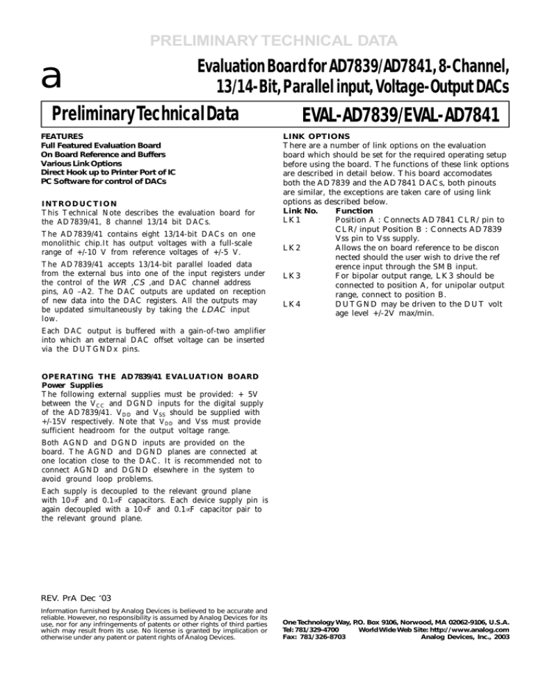
PRELIMINARY TECHNICAL DATA a Evaluation Board for AD7839/AD7841, 8-Channel, 13/14-Bit, Parallel input, Voltage-Output DACs Preliminary Technical Data FEATURES Full Featured Evaluation Board On Board Reference and Buffers Various Link Options Direct Hook up to Printer Port of IC PC Software for control of DACs INTRODUCTION This Technical Note describes the evaluation board for the AD7839/41, 8 channel 13/14 bit DACs. The AD7839/41 contains eight 13/14-bit DACs on one monolithic chip.It has output voltages with a full-scale range of +/-10 V from reference voltages of +/-5 V. The AD7839/41 accepts 13/14-bit parallel loaded data from the external bus into one of the input registers under the control of the WR ,CS ,and DAC channel address pins, A0 –A2. The DAC outputs are updated on reception of new data into the DAC registers. All the outputs may be updated simultaneously by taking the LDAC input low. EVAL-AD7839/EVAL-AD7841 LINK OPTIONS There are a number of link options on the evaluation board which should be set for the required operating setup before using the board. The functions of these link options are described in detail below. This board accomodates both the AD7839 and the AD7841 DACs, both pinouts are similar, the exceptions are taken care of using link options as described below. Link No. Function LK1 Position A : Connects AD7841 CLR/ pin to CLR/ input Position B : Connects AD7839 Vss pin to Vss supply. Allows the on board reference to be discon nected should the user wish to drive the ref erence input through the SMB input. For bipolar output range, LK3 should be connected to position A, for unipolar output range, connect to position B. DUTGND may be driven to the DUT volt age level +/-2V max/min. LK2 LK3 LK4 Each DAC output is buffered with a gain-of-two amplifier into which an external DAC offset voltage can be inserted via the DUTGNDx pins. OPERATING THE AD7839/41 EVALUATION BOARD Power Supplies The following external supplies must be provided: + 5V between the VCC and DGND inputs for the digital supply of the AD7839/41. VDD and VSS should be supplied with +/-15V respectively. Note that VDD and Vss must provide sufficient headroom for the output voltage range. Both AGND and DGND inputs are provided on the board. The AGND and DGND planes are connected at one location close to the DAC. It is recommended not to connect AGND and DGND elsewhere in the system to avoid ground loop problems. Each supply is decoupled to the relevant ground plane with 10µF and 0.1µF capacitors. Each device supply pin is again decoupled with a 10µF and 0.1µF capacitor pair to the relevant ground plane. REV. PrA Dec ‘03 Information furnished by Analog Devices is believed to be accurate and reliable. However, no responsibility is assumed by Analog Devices for its use, nor for any infringements of patents or other rights of third parties which may result from its use. No license is granted by implication or otherwise under any patent or patent rights of Analog Devices. One Technology Way, P.O. Box 9106, Norwood, MA 02062-9106, U.S.A. Tel: 781/329-4700 World Wide Web Site: http://www.analog.com Fax: 781/326-8703 Analog Devices, Inc., 2003 PRELIMINARY TECHNICAL DATA EVAL-AD7839/EVAL-AD7841 EVALUATION BOARD SOFTWARE Software Installation The AD7839/41 evaluation kit consists of self-installing software on CD-ROM. In the event of the setup file not running automatically, run the file setup.exe from the CD-ROM. Software is compatible with Win95 to Windows2000. Ensure that the Centronics cable connects the PC to the AD7839/41 eval board. Run the executable file from the Analog Devices Menu. The main screen with drop down menus (File, Printer Port and Help) looks as follows: To update a particular DAC, select the DAC channel, enter the DAC word and click “Update DAC” button. –2– REV. PrA PRELIMINARY TECHNICAL DATA EVAL-AD7839/EVAL-AD7841 Component Listing Name C1 C2 C3 C4 C5 C6 C7 C9 C10 C11 C12 C13 C16 C18 C19 C20 C21 C22 C23 C24 C25 C26 C27 J1 J2 J3 J4 J5 J6 J7 J8 J9 J10 J11 J12 J31 J32 LK1 LK2 LK3 LK4 R1 R2 R3 R4 R5 R6 R7 R8 T1 T2 T3 T4 T5 T6 T7 T8 T9 T10 U1 U2 U3 U4 U5 U6 U7 REV. PrA Part Type CAP CAP+ CAP CAP+ CAP CAP+ CAP CAP CAP CAP+ CAP CAP+ CAP CAP CAP+ CAP CAP+ CAP CAP CAP CAP CAP CAP CENTRONICS SMB SMB SMB SMB SMB SMB SMB SMB SMB SMB SMB CON\POWER CON\POWER3 JUMPER2\SIP3 JUMPER JUMPER2\SIP3 JUMPER RES RES RES RES RES RES RES RES TESTPOINT TESTPOINT TESTPOINT TESTPOINT TESTPOINT TESTPOINT TESTPOINT TESTPOINT TESTPOINT TESTPOINT AD7841_39 74HCT573 74HCT573 74HCT573 ADR02 ADR02 OP1177 Value 0.1uF 10uF 0.1uF 10uF 0.1uF 10uF 0.1uF 0.1uF 0.1uF 10uF 0.1uF 10uF 0.1uF Part Description 16V DC X7R Ceramic Capacitor 10V DC Tantalum Capacitor 16V DC X7R Ceramic Capacitor 20V DC Tantalum Capacitor 16V DC X7R Ceramic Capacitor 20V DC Tantalum Capacitor 16V DC X7R Ceramic Capacitor 16V DC X7R Ceramic Capacitor 16V DC X7R Ceramic Capacitor 20V DC Tantalum Capacitor 16V DC X7R Ceramic Capacitor 20V DC Tantalum Capacitor 16V DC X7R Ceramic Capacitor 10uF 0.1uF 10uF 0.1uF 0.1uF 0.1uF 0.1uF ??? ??? 20V DC Tantalum Capacitor 16V DC X7R Ceramic Capacitor 20V DC Tantalum Capacitor 16V DC X7R Ceramic Capacitor 16V DC X7R Ceramic Capacitor 16V DC X7R Ceramic Capacitor 16V DC X7R Ceramic Capacitor Load Capacitor Load Capacitor 36 Pin 90° Centronics Connector SMB Jack SMB Jack SMB Jack SMB Jack SMB Jack SMB Jack SMB Jack SMB Jack SMB Jack SMB Jack SMB Jack 2 Pin Terminal Block 3 Pin Terminal Block Left for AD7841 - right for AD7839 2 Pin Header 3 Pin Header 2 Pin Header 0.063W Resistor 0.063W Resistor 0.063W Resistor 0.063W Resistor 0.063W Resistor 0.063W Resistor Load Resistor Load Resistor Testpoint Testpoint Testpoint Testpoint Testpoint Testpoint Testpoint Testpoint Testpoint Testpoint 13/14 Bit Parallel Input Voltage Output DAC Octal D-Type Transparent Latch Octal D-Type Transparent Latch Octal D-Type Transparent Latch 5V Reference 5V Reference Precision, Low Loise, Single OP Amp 10k 10k 10k 10k 10k 10k –3– Stock Code FEC 432-210 FEC 197-130 FEC 432-210 FEC 355-2512 FEC 432-210 FEC 355-2512 FEC 432-210 FEC 432-210 FEC 432-210 FEC 355-2512 FEC 432-210 FEC 355-2512 FEC 432-210 Not inserted FEC 355-2512 FEC 432-210 FEC 355-2512 FEC 432-210 FEC 432-210 FEC 432-210 FEC 432-210 FEC 147-753 FEC 410-8164 FEC 410-8164 FEC 410-8164 FEC 410-8164 FEC 410-8164 FEC 410-8164 FEC 410-8164 FEC 410-8164 FEC 410-8164 FEC 410-8164 FEC 410-8164 FEC 151-785 FEC 151-786 FEC 511-717 & 150-411 FEC 511-705 & 150-411 FEC 511-717 & 150-411 FEC 511-705 & 150-411 FEC 911-355 FEC 911-355 FEC 911-355 FEC 911-355 FEC 911-355 FEC 911-355 FEC 240-345 FEC 240-345 FEC 240-345 FEC 240-345 FEC 240-345 FEC 240-345 FEC 240-345 FEC 240-345 FEC 240-345 FEC 240-345 AD7839AS / AD7841AS FEC 492-097 FEC 492-097 FEC 492-097 ADR02AR ADR02AR OP1177AR PRELIMINARY TECHNICAL DATA EVAL-AD7839/EVAL-AD7841 –4– REV. PrA PRELIMINARY TECHNICAL DATA EVAL-AD7839/EVAL-AD7841 REV. PrA –5– PRELIMINARY TECHNICAL DATA EVAL-AD7839/EVAL-AD7841 –6– REV. PrA


