Evaluation Board User Guide UG-184
advertisement
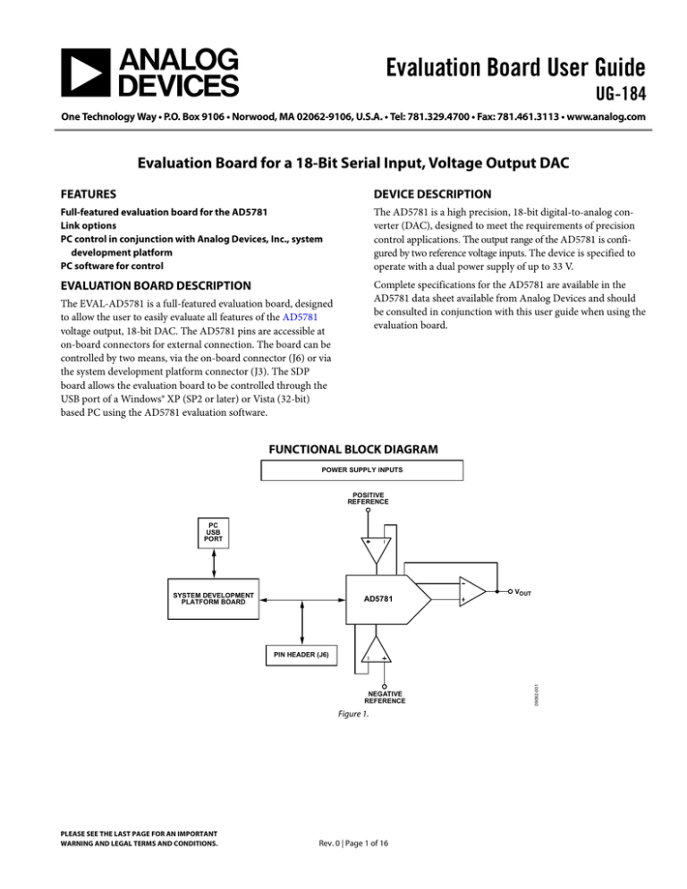
Evaluation Board User Guide UG-184 One Technology Way • P.O. Box 9106 • Norwood, MA 02062-9106, U.S.A. • Tel: 781.329.4700 • Fax: 781.461.3113 • www.analog.com Evaluation Board for a 18-Bit Serial Input, Voltage Output DAC FEATURES DEVICE DESCRIPTION Full-featured evaluation board for the AD5781 Link options PC control in conjunction with Analog Devices, Inc., system development platform PC software for control The AD5781 is a high precision, 18-bit digital-to-analog converter (DAC), designed to meet the requirements of precision control applications. The output range of the AD5781 is configured by two reference voltage inputs. The device is specified to operate with a dual power supply of up to 33 V. EVALUATION BOARD DESCRIPTION Complete specifications for the AD5781 are available in the AD5781 data sheet available from Analog Devices and should be consulted in conjunction with this user guide when using the evaluation board. The EVAL-AD5781 is a full-featured evaluation board, designed to allow the user to easily evaluate all features of the AD5781 voltage output, 18-bit DAC. The AD5781 pins are accessible at on-board connectors for external connection. The board can be controlled by two means, via the on-board connector (J6) or via the system development platform connector (J3). The SDP board allows the evaluation board to be controlled through the USB port of a Windows® XP (SP2 or later) or Vista (32-bit) based PC using the AD5781 evaluation software. FUNCTIONAL BLOCK DIAGRAM POWER SUPPLY INPUTS POSITIVE REFERENCE PC USB PORT SYSTEM DEVELOPMENT PLATFORM BOARD AD5781 VOUT NEGATIVE REFERENCE Figure 1. PLEASE SEE THE LAST PAGE FOR AN IMPORTANT WARNING AND LEGAL TERMS AND CONDITIONS. Rev. 0 | Page 1 of 16 09092-001 PIN HEADER (J6) UG-184 Evaluation Board User Guide TABLE OF CONTENTS Features .............................................................................................. 1 Evaluation Board Software ...............................................................5 Evaluation Board Description......................................................... 1 Software Installation .....................................................................5 Device Description ........................................................................... 1 Software Operation .......................................................................5 Functional Block Diagram .............................................................. 1 Main Window ................................................................................6 Revision History ............................................................................... 2 Evaluation Board Performance........................................................8 Evaluation Board Hardware ............................................................ 3 Evaluation Board Schematics and Artwork ...................................9 Power Supplies .............................................................................. 3 Ordering Information .................................................................... 15 Link Options ................................................................................. 3 Bill of Materials ........................................................................... 15 On-Board Connectors ................................................................. 3 REVISION HISTORY 8/10—Revision 0: Initial Version Rev. 0 | Page 2 of 16 Evaluation Board User Guide UG-184 EVALUATION BOARD HARDWARE POWER SUPPLIES Connector J6 Pin Descriptions The following external supplies must be provided: Table 2. Connector J6 Pin Configuration • 9 10 • • 5 V between the VCC and DGND inputs for the digital supply of the AD5781. Alternatively, place Link 1 in Position A to power the digital circuitry from the USB port (default). 7.5 V to 16.5 V between the VDD and AGND inputs for the positive analog supply of the AD5781. −2.5 V to −16.5 V between the VSS and AGND inputs for the negative analog supply of the AD5781. The analog and digital planes are connected at one location, close to the AD5781. To avoid ground loop problems, it is recommended not to connect AGND and DGND elsewhere in the system. Each supply is decoupled to the relevant ground plane with 10 μF and 0.1 μF capacitors. Each device supply pin is again decoupled with a 10 μF and 0.1 μF capacitor pair to the relevant ground plane. 7 8 5 6 3 4 1 2 Table 3. Connector J6 Pin Descriptions Pin No. 1 2 3 4 5 6 7 8 9 10 Description SDO RESET DGND CLR IOVCC LDAC SDIN DGND SCLK SYNC LINK OPTIONS ON-BOARD CONNECTORS The link options on the evaluation board should be set for the required operating setup before using the board. The functions of the link options are described in Table 5. There are nine connectors on the AD5781 evaluation board PCB as outlined in Table 4. Default Link Option Setup The default link options are listed in Table 1. Table 1. Default Link Options Link No. LK1 LK3 LK4 LK5 LK6 LK8 LK9 Option A A Removed Removed Removed A C Table 4. On-Board Connectors Connector J1 J2 J3 J6 VOUT VOUT_BUF VREF VREFN VREFP Rev. 0 | Page 3 of 16 Function Analog power supply connector Digital power supply connector SDP board connector Digital interface pin header connector DAC output connector Buffered DAC output connector 5 V voltage reference input connector (+10 V and −10 V reference voltages are generated from 5 V input) DAC negative reference input connector DAC positive reference input connector UG-184 Evaluation Board User Guide Table 5. Link Options Link No. LK1 LK3 LK4 Description This link selects the source of the digital power supply. Position A selects the source from the SDP board. Position B selects the source from Connector J2. This link selects the voltage source for the IOVCC pin. Position A connects IOVCC to VCC. Position B selects an externally applied voltage at Pin 5 of J6. This link selects the state of the LDAC pin. When this link is inserted, LDAC is at logic low. When this link is removed, LDAC is at logic high. LK5 This link selects the state of the CLR pin. When this link is inserted, CLR is at logic low. When this link is removed, CLR is at logic high. LK6 This link selects the state of the RESET pin. When this link is inserted, RESET is at logic low. When this link is removed, RESET is at logic high. LK8 This link selects the positive reference source. Position A selects an on-board generated 10 V, derived from 5 V applied at Connector VREF. Position B selects an external voltage applied at Connector VREFP. This link selects the negative reference source. Position A selects an external voltage applied at Connector VREFN. Position B selects AGND. Position C selects an on-board generated −10 V, derived from 5 V applied at Connector VREF. LK9 Rev. 0 | Page 4 of 16 Evaluation Board User Guide UG-184 EVALUATION BOARD SOFTWARE SOFTWARE INSTALLATION SOFTWARE OPERATION The AD5781 evaluation kit includes self-installing software on a CD. The software is compatible with Windows XP (SP2) and Vista (32-bit). If the setup file does not run automatically, you can run setup.exe from the CD. To launch the software, complete the following steps: Install the evaluation software before connecting the evaluation board and SDP board to the USB port of the PC to ensure that the evaluation system is correctly recognized when connected to the PC. 2. If the evaluation system is not connected to the USB port when the software is launched, a connectivity error is displayed (see Figure 2). Connect the evaluation board to the USB port of the PC, wait a number of seconds, and click Rescan. Follow the instructions. After installation from the CD is complete, power up the AD5781 evaluation board as described in the Power Supplies section. Connect the SDP board (Connector A) to the AD5781 evaluation board and then to the USB port of your PC using the supplied cable. When the evaluation system is detected, proceed through any dialog boxes that appear. This completes the installation. 09092-002 2. From the Start menu, select Analog Devices – AD5781 > AD5781 Evaluation Software. The main window of the software is displayed (see Figure 3). Figure 2. Connectivity Error Alert 09092-003 1. 1. Figure 3. Main Window Rev. 0 | Page 5 of 16 UG-184 Evaluation Board User Guide To begin the measurement, click the START button. The measurement can be halted at anytime by clicking the STOP button. When the measurement is completed, a dialog box appears to allow the data to be saved as a spreadsheet file with three columns of data. The first column is DAC code, the second column is DAC voltage in volts, and the third column is INL error in LSBs, as shown in Figure 5. A graph of both DAC output voltage vs. DAC code and INL error vs. DAC code is displayed on-screen (see Figure 6). In the measurement example shown in Figure 6 measurements are taken in 256 code steps beginning at Code 0 and finishing at Code 261,888, in total 1023 measurements. With the number of power line cycles (NPLC) setting on the multimeter set to 1, the measurement takes ~75 sec to complete. To complete an all codes measurement requiring 262,144 measurement points takes ~6 hours to complete. MAIN WINDOW The main window is divided into three tabs: Configure, Program Voltage, and Measure DAC Output. Configure The Configure section allows access to the control register, clearcode register, software control register, and DAC register and also allows control of the RESET, CLR, and LDAC pins. Program Voltage 09092-004 The Program Voltage section programs the DAC register with a value calculated from the entered values: the positive voltage reference (VREFP), the negative voltage reference (VREFN), and the desired output voltage (see Figure 4). Figure 4. Program Voltage Window Measure DAC Output The multimeter is controlled over a general-purpose interface bus (GPIB). Once connected to the PC, the multimeter should first be configured via its front panel before taking a measurement. Figure 6 shows the measurement options. The software runs through a sequence of steps, programming the DAC register and measuring the DAC output voltage. The sequence begins with the software programming the DAC with the Start Code value, incrementing the programmed value at each step by the Code Step value, and finishing when the programmed value reaches the Stop Code value. A delay between measurements can be inserted if required. The GPIB address of the multimeter must be specified. 09092-006 The Measure DAC Output section allows the PC to control an Agilent 3458A multimeter to measure and log the DAC output voltage. Figure 5. Saved Data Format If an Agilent 3458A multimeter is not connected to the PC, the software steps through the codes without taking any measurements. Rev. 0 | Page 6 of 16 UG-184 09092-005 Evaluation Board User Guide Figure 6. Measure DAC Output Window Rev. 0 | Page 7 of 16 UG-184 Evaluation Board User Guide EVALUATION BOARD PERFORMANCE The following data demonstrates the measured linearity performance of the AD5781 evaluation board circuit. The board is powered from VDD = +15 V, VSS = −15 V, and VREF = +5 V. 0.5 0.4 0.3 INL ERROR (LSB) 0.2 0.1 0 –0.1 –0.2 –0.3 –0.5 0 50k 100k 150k 200k 250k DAC CODE 09092-007 –0.4 Rev. 0 | Page 8 of 16 262,143 240k 09092-008 DAC CODE Figure 8. DNL Error vs. DAC Code 220k 200k 180k 160k 140k 120k 80k 100k 60k 40k 20k 0.50 0.45 0.40 0.35 0.30 0.25 0.20 0.15 0.10 0.05 0 –0.05 –0.10 –0.15 –0.20 –0.25 –0.30 –0.35 –0.40 –0.45 –0.50 0 DNL ERROR (LSBs) Figure 7. INL Error vs. DAC Code Evaluation Board User Guide UG-184 EVALUATION BOARD SCHEMATICS AND ARTWORK 09092-009 Figure 9. Schematic of the AD5781 Circuitry Rev. 0 | Page 9 of 16 Evaluation Board User Guide 09092-010 UG-184 Figure 10. Schematic of the Voltage Reference Scaling Circuitry Rev. 0 | Page 10 of 16 UG-184 09092-011 Evaluation Board User Guide Figure 11. Schematic of the SDP Board Connector Rev. 0 | Page 11 of 16 Evaluation Board User Guide 09092-012 UG-184 09092-013 Figure 12. Component Placement Schematic Figure 13. Top PCB Layer Schematic Rev. 0 | Page 12 of 16 UG-184 09092-014 Evaluation Board User Guide 09092-015 Figure 14. Inner First PCB Layer Schematic Figure 15. Inner Second PCB Layer Schematic Rev. 0 | Page 13 of 16 Evaluation Board User Guide 09092-016 UG-184 Figure 16. Bottom PCB Layer Schematic Rev. 0 | Page 14 of 16 Evaluation Board User Guide UG-184 ORDERING INFORMATION BILL OF MATERIALS Table 6. Reference Designator C1, C2, C9, C11, C12, C16, C17, C20, C41, C42, C48, C54, C95, C96, C98, C99, C102, C103 C3, C4, C5, C6, C7, C8, C10, C25, C31, C40, C43, C45, C47, C53, C93, C100, C101 J1 J2 J3 J6 L1, L2, L3, L4 LK1, LK3 LK4, LK5, LK6 LK8, LK9 R1, R2, R3, R4, R5, R6, R7 R8 R15, R16, R17, R18 R45, R46, R47 R48 TP1 to TP7 U2 U3 U6 U8 U11 U28 VOUT, VOUT_BUF, VREF, VREFN, VREFP Part Description Capacitor, 10 μF, 16 V, 10%, Case B Part Number TAJB106K016R Stock Code FEC 498737 Capacitor, 0603, 0.1 μF, 16 V B0603R104KCT FEC 9406140 3-pin terminal block (5 mm pitch) 2-pin terminal block (5 mm pitch) 120-way connector (0.6 mm pitch) 20-pin (2 × 10) header Ferrite bead 600 Ω 3-pin SIL header and shorting link 2-pin (0.1" pitch) header and shorting shunt 4-pin (2 × 2) 0.1" header and shorting shunt SMD resistor, 0 Ω SMD resistor, 1.5 kΩ SMD resistor, 10 kΩ Precision resistor, 1 kΩ Precision resistor, 2 kΩ Black testpoint Dual op amp 64K I2C serial EEPROM Single op amp, 8-pin Dual op amp 18-bit, ±1 LSB INL, voltage output DAC Single op amp, 8-pin Straight PCB mount SMB jack, 50 Ω CTB5000/3 CTB5000/2 FX8-120S-SV(21) N/A 74279204 M20-9990345 and M7567-05 M20-9990246 and M7566-05 FEC 151790 FEC 151789 FEC 1324660 FEC 1022244 (36 + 36 pin strip) FEC 1635719 FEC 1022248 and FEC 150410 FEC 1022247 and FEC 150-411 M20-9983646 and M7566-05 FEC 1022244 and 150-411 (36 pin strip) FEC 9331662 FEC 9333924 FEC 9331700 FEC 1108863 FEC 1108872 FEC 240-333 AD8676BRZ FEC 9758070 AD8675ARZ AD8676BRZ AD5781BRUZ AD8675ARZ FEC 1206013 MC 0.063W 0603 0R MC 0.1W 0805 5% 1K5 MC 0.063W 0603 10k PCF0805-13-1K-B-T1 PCF0805-13-2K-B-T1 20-2137 AD8676BRZ 24LC64-ISN AD8675ARZ AD8676BRZ AD5781BRUZ AD8675ARZ 1-1337482-0 Rev. 0 | Page 15 of 16 UG-184 Evaluation Board User Guide NOTES ESD Caution ESD (electrostatic discharge) sensitive device. Charged devices and circuit boards can discharge without detection. Although this product features patented or proprietary protection circuitry, damage may occur on devices subjected to high energy ESD. Therefore, proper ESD precautions should be taken to avoid performance degradation or loss of functionality. Legal Terms and Conditions By using the evaluation board discussed herein (together with any tools, components documentation or support materials, the “Evaluation Board”), you are agreeing to be bound by the terms and conditions set forth below (“Agreement”) unless you have purchased the Evaluation Board, in which case the Analog Devices Standard Terms and Conditions of Sale shall govern. Do not use the Evaluation Board until you have read and agreed to the Agreement. Your use of the Evaluation Board shall signify your acceptance of the Agreement. This Agreement is made by and between you (“Customer”) and Analog Devices, Inc. (“ADI”), with its principal place of business at One Technology Way, Norwood, MA 02062, USA. Subject to the terms and conditions of the Agreement, ADI hereby grants to Customer a free, limited, personal, temporary, non-exclusive, non-sublicensable, non-transferable license to use the Evaluation Board FOR EVALUATION PURPOSES ONLY. Customer understands and agrees that the Evaluation Board is provided for the sole and exclusive purpose referenced above, and agrees not to use the Evaluation Board for any other purpose. Furthermore, the license granted is expressly made subject to the following additional limitations: Customer shall not (i) rent, lease, display, sell, transfer, assign, sublicense, or distribute the Evaluation Board; and (ii) permit any Third Party to access the Evaluation Board. As used herein, the term “Third Party” includes any entity other than ADI, Customer, their employees, affiliates and in-house consultants. The Evaluation Board is NOT sold to Customer; all rights not expressly granted herein, including ownership of the Evaluation Board, are reserved by ADI. CONFIDENTIALITY. This Agreement and the Evaluation Board shall all be considered the confidential and proprietary information of ADI. Customer may not disclose or transfer any portion of the Evaluation Board to any other party for any reason. Upon discontinuation of use of the Evaluation Board or termination of this Agreement, Customer agrees to promptly return the Evaluation Board to ADI. ADDITIONAL RESTRICTIONS. Customer may not disassemble, decompile or reverse engineer chips on the Evaluation Board. Customer shall inform ADI of any occurred damages or any modifications or alterations it makes to the Evaluation Board, including but not limited to soldering or any other activity that affects the material content of the Evaluation Board. Modifications to the Evaluation Board must comply with applicable law, including but not limited to the RoHS Directive. TERMINATION. ADI may terminate this Agreement at any time upon giving written notice to Customer. Customer agrees to return to ADI the Evaluation Board at that time. LIMITATION OF LIABILITY. THE EVALUATION BOARD PROVIDED HEREUNDER IS PROVIDED “AS IS” AND ADI MAKES NO WARRANTIES OR REPRESENTATIONS OF ANY KIND WITH RESPECT TO IT. ADI SPECIFICALLY DISCLAIMS ANY REPRESENTATIONS, ENDORSEMENTS, GUARANTEES, OR WARRANTIES, EXPRESS OR IMPLIED, RELATED TO THE EVALUATION BOARD INCLUDING, BUT NOT LIMITED TO, THE IMPLIED WARRANTY OF MERCHANTABILITY, TITLE, FITNESS FOR A PARTICULAR PURPOSE OR NONINFRINGEMENT OF INTELLECTUAL PROPERTY RIGHTS. IN NO EVENT WILL ADI AND ITS LICENSORS BE LIABLE FOR ANY INCIDENTAL, SPECIAL, INDIRECT, OR CONSEQUENTIAL DAMAGES RESULTING FROM CUSTOMER’S POSSESSION OR USE OF THE EVALUATION BOARD, INCLUDING BUT NOT LIMITED TO LOST PROFITS, DELAY COSTS, LABOR COSTS OR LOSS OF GOODWILL. ADI’S TOTAL LIABILITY FROM ANY AND ALL CAUSES SHALL BE LIMITED TO THE AMOUNT OF ONE HUNDRED US DOLLARS ($100.00). EXPORT. Customer agrees that it will not directly or indirectly export the Evaluation Board to another country, and that it will comply with all applicable United States federal laws and regulations relating to exports. GOVERNING LAW. This Agreement shall be governed by and construed in accordance with the substantive laws of the Commonwealth of Massachusetts (excluding conflict of law rules). Any legal action regarding this Agreement will be heard in the state or federal courts having jurisdiction in Suffolk County, Massachusetts, and Customer hereby submits to the personal jurisdiction and venue of such courts. The United Nations Convention on Contracts for the International Sale of Goods shall not apply to this Agreement and is expressly disclaimed. ©2010 Analog Devices, Inc. All rights reserved. Trademarks and registered trademarks are the property of their respective owners. UG09092-0-8/10(0) Rev. 0 | Page 16 of 16
