a Engineer-to-Engineer Note EE-176
advertisement

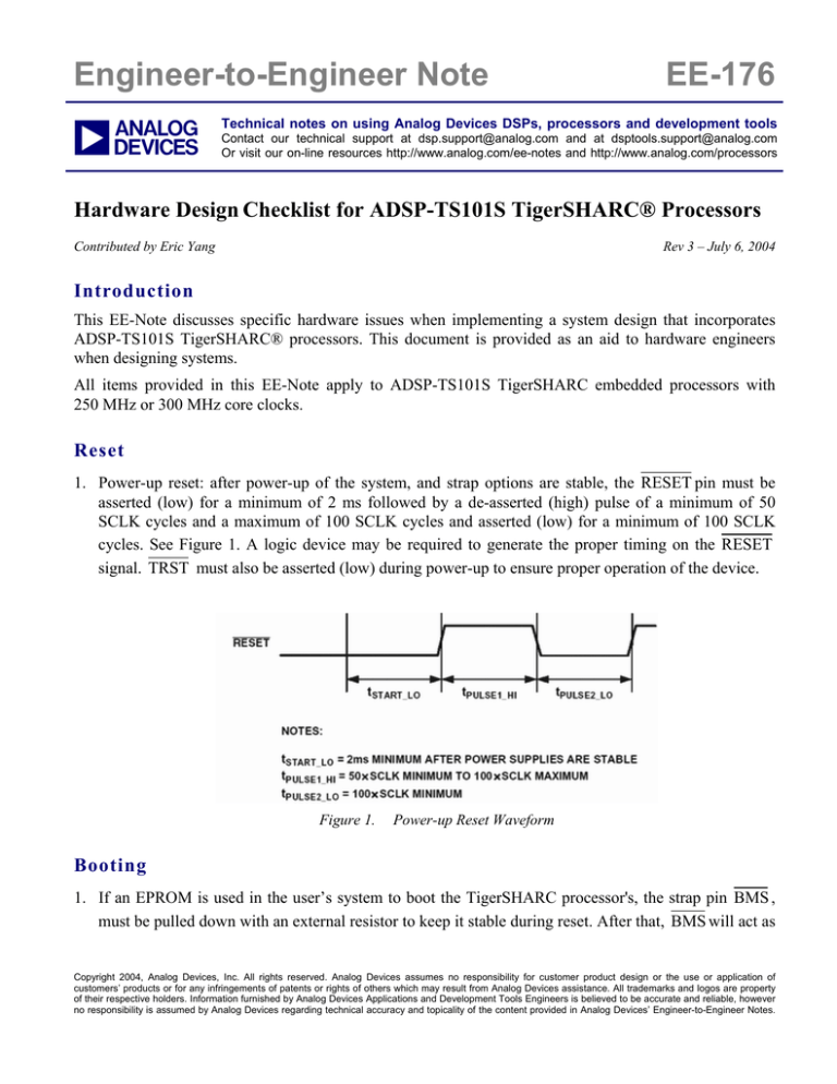
Engineer-to-Engineer Note a EE-176 Technical notes on using Analog Devices DSPs, processors and development tools Contact our technical support at dsp.support@analog.com and at dsptools.support@analog.com Or visit our on-line resources http://www.analog.com/ee-notes and http://www.analog.com/processors Hardware Design Checklist for ADSP-TS101S TigerSHARC® Processors Contributed by Eric Yang Rev 3 – July 6, 2004 Introduction This EE-Note discusses specific hardware issues when implementing a system design that incorporates ADSP-TS101S TigerSHARC® processors. This document is provided as an aid to hardware engineers when designing systems. All items provided in this EE-Note apply to ADSP-TS101S TigerSHARC embedded processors with 250 MHz or 300 MHz core clocks. Reset 1. Power-up reset: after power-up of the system, and strap options are stable, the RESET pin must be asserted (low) for a minimum of 2 ms followed by a de-asserted (high) pulse of a minimum of 50 SCLK cycles and a maximum of 100 SCLK cycles and asserted (low) for a minimum of 100 SCLK cycles. See Figure 1. A logic device may be required to generate the proper timing on the RESET signal. TRST must also be asserted (low) during power-up to ensure proper operation of the device. Figure 1. Power-up Reset Waveform Booting 1. If an EPROM is used in the user’s system to boot the TigerSHARC processor's, the strap pin BMS , must be pulled down with an external resistor to keep it stable during reset. After that, BMS will act as Copyright 2004, Analog Devices, Inc. All rights reserved. Analog Devices assumes no responsibility for customer product design or the use or application of customers’ products or for any infringements of patents or rights of others which may result from Analog Devices assistance. All trademarks and logos are property of their respective holders. Information furnished by Analog Devices Applications and Development Tools Engineers is believed to be accurate and reliable, however no responsibility is assumed by Analog Devices regarding technical accuracy and topicality of the content provided in Analog Devices’ Engineer-to-Engineer Notes. a the EPROM chip select signal. If EPROM is not used, pull up this pin with a 10KΩ resistor or tie it directly to VDD_IO. 2. ADSP-TS101S processors have three boot modes — EPROM, host, and link port. Refer to [5] “ADSP-TS101S TigerSHARC Processor Boot Loader Kernels Operation (EE-174)” and the source code files under “..\Analog Devices\VisualDSP\Ts\ldr” to learn the whole process. Select one of the modes to boot the TigerSHARC processors in your system. Clock 1. Derive SCLK and LCLK from the same clock source. 2. If the system must work deterministically cycle-by-cycle, use an integer LCLK multiplication (2, 3, 4, 5, or 6) when setting LCLKRAT. Otherwise, a non-integer multiplier will also be fully functional and perfectly acceptable. 3. The maximum LCLK/SCLK input jitter tolerance is 100 ps. Refer to the IDT® (www.idt.com) or Cypress® (www.cypress.com) Web site to choose a proper clock buffer (TurboClock™ 1 or RoboClock™ 2). 4. All ADSP-TS101S processors in a cluster (and any devices that interface an ADSP-TS101S in a synchronous manner) should use the following guidelines. • Provide a single clock source for each fan-out buffer. Never mix frequencies. Refer to Figure 2. Cl ock buf f er wi t h mul t i r ef er ence i nput s Cl ock sour ces of di f f er ent f r equenci es Cl ock sour ce 1 Cl ock buf f er wi t h mul t i r ef er ence i nput s ... ... Cl ock sour ce 1 ... ... Cl ock sour ce 2 ... Cl ock sour ce Cl ock sour ce 2 ... Bad Good Figure 2. • Cl ock buf f er s wi t h si ngl e r ef er ence i nput Using fan-out buffers Connections should be point-to-point from zero-skew clock buffer output to device clock input. Match trace lengths to minimize skew. See Figure 3. 1 TurboClock™ is the trademark of IDT®. 2 RoboClock™ is the trademark of Cypress®. Hardware Design Checklist for ADSP-TS101S TigerSHARC® Processors (EE-176) Page 2 of 11 Cl ust er Bus a Zer o- skew cl ock buf f er Ti ger SHARC ( I D=0) Ti ger SHARC ( I D=1) ... ... Ti ger SHARC ( I D=N) Cl ock Sour ce Synchr onous Host SDRAM ... Ot her Synchr onous Memor y or Devi ces These cl ocks shoul d be dr i ven poi nt t o poi nt , and t r ace l engt hs shoul d be mat ched. Figure 3. Clock distribution method Power Supply 10uH VDD VDDA VDDA 1uF 1nF Ti ger SHARC 1. Note that the analog supply (VDD_A) provides power to the clock generator PLLs. To produce a stable clock, systems must provide a clean power supply to power input VDD_A. Designers must pay critical attention to bypassing the VDD_A supply. Figure 4 is a reference design of the filtering circuit. Place components as close as possible to the device. 10uH VSSA VSSA Figure 4. Analog power supply filtering circuit reference design 2. The required power-on sequence for the DSP is to provide VDD (and VDD_A) before VDD_IO. 3. Ensure that the proper DC/DC module is chosen to provide the right voltage and enough current to the core and I/O part of TigerSHARC. Refer to [4] “Estimating Power For The ADSP-TS101S (EE-169)” to learn the method of power dissipation calculation. Consider the worst case. 4. Place bypass caps on the bottom side of the board, as close to the power pins as possible. There are several ways to achieve this. Hardware Design Checklist for ADSP-TS101S TigerSHARC® Processors (EE-176) Page 3 of 11 a • 0.1uF low-inductance caps are recommended for bypass. 0.01uF and 0.001uF capacitors can also be used with the 0.1uF capacitors for higher frequency filtering, provided their inductance is small enough. In some cases SPICEing of the power supply filtering characteristics may be necessary. • Use blind vias from the package balls to create sufficient space for capacitor placement. The disadvantage to this is that blind vias are more expensive and that blind vias are not accessible for scope probes. • Part the traces in the four quadrants of the chip in four opposite directions, as shown in Figure 5. Use the two resulting open horizontal and vertical lanes for placing SMD capacitors of size 0402 or smaller. The disadvantage is that small capacitor packages may be difficult to handle. Figure 5. Bypass capacitors layout scheme 5. Enough bulk capacitors are used to prevent voltage vibration on power supply plane caused by great current variation. Several parallel electrolytic and tantalum capacitors are preferred in order to provide high capacitance and low ESR. JTAG Port 1. In a multiprocessor system, use separate buffers to drive the TCKs of different TigerSHARC processors in order to get monotonic rising edges on these pins. For detailed and updated information, refer to [6] “Analog Devices JTAG Emulation Technical Reference(EE-68)”. 2. Ensure that there is enough keep-out space around the JTAG connector so that the JTAG pod can be easily plugged onto the board. For detailed and updated information, refer to [6] “Analog Devices JTAG Emulation Technical Reference (EE-68)”. Hardware Design Checklist for ADSP-TS101S TigerSHARC® Processors (EE-176) Page 4 of 11 a Strap Pins 1. Ensure that all strap pins are set to the desired state during reset. Signal EBOOT On Pin BMS Description EPROM boot. 0 = boot from EPROM immediately after reset (default) 1 = idle after reset and wait for an external device to boot DSP through the external port or a link port IRQEN BM Interrupt Enable. 0 = disable and set IRQ[3 : 0] interrupts to level-sensitive after reset (default) 1 = enable and set IRQ[3 : 0] interrupts to edge-sensitive immediately after reset TM1 L2DIR Test Mode 1. 0 = required setting during reset. 1 = reserved. TM2 TMR0E Test Mode 2. 0 = required setting during reset. 1 = reserved. Table 1. Strap pins definition Cluster Bus 1. Set single-processor ID as “000”. Set multiprocessor IDs as “000” to “N-1”, where N is the number of TigerSHARC processors on the same cluster bus (N=1, 2, ... , 8). Set the ID pins properly. 2. If there is a host on the cluster bus and common data are shared between the host and the TigerSHARC processor, match the endianess on two sides to each other. 3. Connect the address bus in a proper way. Since the TigerSHARC processor’s addressing is wordoriented and most host processors’ addressing are byte-oriented, do not connect the LS-bit of TigerSHARC’s address bus to the LS-bit of the host’s address bus, instead, connect to its the 3rd LSbit, regardless whether a 32-bit or a 64-bit bus width is applied. 4. The address and data buses may float for several cycles during bus mastership transitions between a TigerSHARC and a host. "Floating" means that these inputs are not driven by any source and that DCbiased terminations are not present. It is not necessary to add pull-up resistors as there are no reliability issues and the worst-case power consumption for these floating inputs is negligible. Unconnected address pins may require pull-up or pull-down resistors to avoid erroneous slave accesses, depending on the system. Unconnected data pins may be left floating. 5. If the host or memory bus width is 64 bits, multiprocessing must also be 64 bits. Hardware Design Checklist for ADSP-TS101S TigerSHARC® Processors (EE-176) Page 5 of 11 a 6. If an external wait state is used, ensure that contention on ACK signal will not be caused. To solve this problem, refer to [1] “ADSP-TS101 TigerSHARC Processor Hardware Reference”. 7. If SDRAM is connected on the cluster bus, the address pins connection between these two devices may vary because of the different bus width and memory size. Refer to [1] “ADSP-TS101 TigerSHARC Processor Hardware Reference”. 8. If FLYBY write transaction is used to move data directly from I/O to memory, use IOEN to enable the output buffer of the I/O device. 9. External slave devices de-assert ACK to add wait states to external memory accesses. The ADSPTS101S can de-assert ACK to add wait states to read accesses of its internal memory, but it does not drive ACK during slave writes. Therefore, an external (approximately 10KΩ) pull-up is required. 10. If the fly-by DMA is used, ensure that the R/W timing of the external memory and the I/O device are matched. 11. If designers want to use ZBT-SRAM in their system, remember that only the flow-through ZBTSRAMs can be connected gluelessly, but not pipelined ZBT-SRAMs. This is because when TigerSHARC accesses the cluster bus using pipelined protocol, the write pipeline depth is fixed as 1, the same as flow-through ZBT-SRAMs. The write pipeline depth of pipelined ZBT-SRAMs is fixed as 2, which is incompatible with TigerSHARC processors. 12. In a multiprocessor system, if there are fewer than 8 TigerSHARCs on the same cluster bus, de-assert any unused BRx or HBR (i.e., pull up to VDD_IO with a resistor). 13. Pay great attention to the signal integrity on cluster bus in a multiprocessor system. The SI analysis must be performed in such case. Designers can find the ibis model file on ADI’s Web site. Link Ports 1. Ensure that all link port signals have the same routing delay. If buffers are used, as shown in Figure 1, ensure that all the buffers have almost the same delay for synchronization consideration, especially if a backplane or cable connection is used. 2. If buffers are used, to prevent contention on LxDAT wires, the buffers must be disabled during reset, since the LxDIRs are three-stated when RESET is asserted. If the buffers are enabled but the LxDIRs are three-stated, the two buffers on both sides may drive the wires between them at the same time, potentially causing a large current from VDD_IO to ground. 3. Because internal-to-internal DMA is not supported by the ADSP-TS101S hardware, directly, you may connect two unused link ports together and copy memory through this loop-back by using the respective transmit and receive link port DMA channels. 4. LxCLKIN pins should be pulled up to VDD_IO to prevent spurious noise from triggering link port DMA transfers corrupting ADSP-TS101 memory. This corruption may happen during the time between reset signal deassertion and disabling unused linkport/DMA channels in boot kernel code or in application code because all 4 linkport/DMA receive channels are enabled by default regardless of booting mode. The only case in which external pullups aren't needed is when there is a link port connection between 2 ADSP-TS101's that share a common reset signal, because the TS101 will drive these pins to stable state right after reset. Hardware Design Checklist for ADSP-TS101S TigerSHARC® Processors (EE-176) Page 6 of 11 a The pull up resistors may be 10Kohm, but tests should be performed to find the ideal value for a particular board. They must be placed very closed to the device in order to avoid reflection glitches. In all cases, if a link port is not used for boot, its controls and its DMA must be disabled as soon as possible after boot to avoid spurious transfers that may corrupt the memory. LxCLKIN LxCLKIN LxCLKOUT LxDAT LxCLKOUT 8 LxDAT Minimal link - no buffering LxCLKIN LxCLKIN LxCLKOUT LxDAT LxCLKOUT 8 LxDIR LxDAT LxDIR Buffered link - using LxDIR Figure 6. Buffered link port configuration Hardware Design Checklist for ADSP-TS101S TigerSHARC® Processors (EE-176) Page 7 of 11 a Miscellaneous Items 1. Connect VREF, LCLK_N, and SCLK_N to a reference voltage of 1.5V±100mV. Figure 7 shows a possible filtering circuit. Figure 7. VREF, SCLKN and LCLKN filtering scheme 2. Since control impedance and drive strength of the I/O pins can be adjusted by the pull-up or pull-down resistors on CONTROLIMP[2:0] and DS[2:0] pins, configure these pins in the most proper way according to the result of signal integrity analysis. If SI analysis is impossible, use switches or jumpers to select between pull-ups and pull-downs (or just populate the resistors in different ways to obtain the best signal integrity if SI analysis is impossible). See Figure 8. VDD_I O VDD_I O TS101S TS101S CONTROLI MP0 CONTROLI MP0 CONTROLI MP1 CONTROLI MP1 CONTROLI MP2 CONTROLI MP2 DS0 DS0 DS1 DS1 DS2 DS2 Onl y popul at e one of t he r esi st or s connect ed t o each pi n Use swi t ches or j umper s t o sel ect bet ween pul l ups and pul l downs Figure 8. Drive strength configuration methods Hardware Design Checklist for ADSP-TS101S TigerSHARC® Processors (EE-176) Page 8 of 11 a 3. Internal pull-ups or pull-downs are too weak to be relied on. Use external pull-ups or pull-downs to keep the bi-directional and input pins in de-asserted state should these pins be unused in your system or during transient time between drivers. Unused Inputs Unused Outputs Pins that must be connected Pins Handling Method Pins Handling Method Pins Addr31-0 Data63-0 /RD /WRL /WRH ACK /BRST /BR7-0 PD NC NC (internal pull-up1) NC (internal pull-up1) NC (internal pull-up1) PU NC (internal pull-up1) PU /MS1-0 /MSH /BUSLOCK /FLYBY /IOEN /LDQM /HDQM /SDA10 /BOFF PU /LxCLKOUT NC NC NC NC NC NC NC NC NC LCLK_N LCLK_P LCLKRAT2-0 SCLK_N SCLK_P SCLKFREQ /RESET CONTROLIMP2-0 DS2-0 /HBR LxDIR NC /BMS3 (Strap – EBOOT) NC /BM3 (Strap – IRQEN) /DPA PU PU for ID7-1, PU or NC for ID0 PU for ID7-1, PU or NC for ID0 PU for ID7-1, PU or NC for ID0 /DMAR3-0 PU /HBG /CPA /MSSD /RAS /EMU2 TMR0E3 (Strap – TM1) L2DIR3 (Strap – TM2) VDD 1 VDD_A 1 VDD_IO 1 NC (internal pull-up ) NC (internal pull-up ) /CAS NC (internal pull-up ) VREF SDCKE NC (internal pull-up1) VSS NC (internal pull-up ) VSS_A FLAG3-0 NC (internal pull-down1) /TRST2 (must be pulsed or held low after power up) /IRQ3-0 NC (internal pull-up1) LxData7-0 NC LxCLKIN PU 2 PU /SDWE TCK TDI2 1 NC (internal pull-up) 2 TMS NC (internal pull-up) NC = No Connection. PU = Pull-up to VDD_IO through 10KΩ resistor is required. PD = Pull-down to VSS through 10KΩ resistor is required. 1 That means there is an internal pull-up or pull-down resistor (100KΩ ±50%) on this pin. 2 For more detailed information, refer to EE-68. 3 Refer to Table 1. Table 2. Handling pins Hardware Design Checklist for ADSP-TS101S TigerSHARC® Processors (EE-176) Page 9 of 11 a 4. According to anomaly #29 of the ADSP-TS101S anomaly list [3], the LDQM and HDQM pins have internal pull-downs instead of pull-ups. If you want to use external pull-ups, you may require stronger pull-up resistors to overcome the internal pull-down resistors. 5. SDCKE pin has internal pull-up or pull-down behavior in different situations. If you want to pull the signal down or up externally , use a stronger pull-down or pull-down resistor to overcome the internal resistor. 6. Connect LEDs to unused flag pins to provide explicit indications of instruction flow or machine status for SW and HW debugging. 7. Provide enough space around the device in case a heat sink is needed. 8. Always review the latest errata. Hardware Design Checklist for ADSP-TS101S TigerSHARC® Processors (EE-176) Page 10 of 11 a References [1] ADSP-TS101 TigerSHARC Processor Hardware Reference. Rev. 1.0, April 2003.Analog Devices Inc. [2] ADSP-TS101S TigerSHARC Embedded Processor Data Sheet. Rev. A. Analog Devices Inc. [3] TigerSHARC Anomaly List for Revision(s) TS101S-0.0, TS101S-0.1, TS101S-02. July 2003. Analog Devices Inc. [4] Estimating Power For The ADSP-TS101S (EE-169). February 2003. Analog Devices Inc. [5] ADSP-TS101S TigerSHARC Processor Boot Loader Kernels Operation (EE-174). April 2003. Analog Devices Inc. [6] Analog Devices JTAG Emulation Technical Reference (EE-68). Rev. 2.6, July 2003. Analog Devices Inc. Document History Version Rev 3 – Description July 06, 2004 by Eric Yang Rev 0.1 – December 04, 2003 by Eric Yang Bullet 4 added in Linkport segment. Title changed from Hardware design checklist for ADSP-TS101S to Hardware Design Checklist for ADSP-TS101S TigerSHARC Processors. Added Introduction section. Modified Table 2: • • Handling method of unused Addr31-0 pins – from NC to PD Handling method of unused LxCLKIN pins – from NC to PU Added section to explain the method to handle LDQM and HDQM pins, according to anomaly list. Added section to explain the method to handle SDCKE pin. Deleted the web links in bullet 13 in Cluster Bus section. Changed the names of reference materials. Several sentences reworded from language perspective. Rev 0.0 – November 09, 2002 by Eric Yang Initial Release Hardware Design Checklist for ADSP-TS101S TigerSHARC® Processors (EE-176) Page 11 of 11


