a ADSP-218xN Family Anomaly List for Revision 3.1, 3.2, and 4.0
advertisement
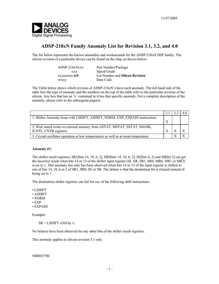
11/07/2005 a Digital Signal Processing ADSP-218xN Family Anomaly List for Revision 3.1, 3.2, and 4.0 The list below represents the known anomalies and workarounds for the ADSP-218xN DSP family. The silicon revision of a particular device can be found on the chip, as shown below: ADSP-218xNxxx -xxx xyzzzzzzz-4.0 wwyy Part Number/Package Speed Grade Lot Number and Silicon Revision Date Code The Table below shows which revision of ADSP-218xN’s have each anomaly. The left hand side of the table lists the type of anomaly and the numbers on the top of the table refer to the particular revision of the silicon. Any box that has an ‘x’ contained in it has that specific anomaly. For a complete description of the anomaly, please refer to the subsequent page(s). 3.1 3.2 4.0 X X X X 1. Shifter Anomaly Issue with LSHIFT, ASHIFT, NORM, EXP, EXPADJ instructions X 2. Wait stated writes to external memory from ASTAT, MSTAT, SSTAT, IMASK, ICNTL, CNTR registers 3. Crystal oscillator operation at low temperatures as well as at room temperature X Anomaly #1: The shifter result registers, SR1[bits 14, 10, 6, 2], SR0[bits 14, 10, 6, 2], SE[bits 6, 2] and SB[bit 2] can get the incorrect result when bits 14 or 13 of the shifter input register (SI, AR, SR1, SR0, MR0, MR1 or MR2) is set to 1. This anomaly has only has been observed when bits 14 or 13 of the input register is shifted to one of bits 14, 10, 6 or 2 of SR1, SR0, SE or SB. The failure is that the destination bit is cleared instead of being set to 1. The destination shifter registers can fail for any of the following shift instructions: • LSHIFT • ASHIFT • NORM • EXP • EXPADJ Example: SR = LSHIFT AX0 by 1; No failures have been observed for any other bits of the shifter result registers. This anomaly applies to silicon revision 3.1 only. NR002578C -1- 11/07/2005 Workaround: 1. This workaround is preliminary and has not been proven to work under all circumstances. Significant testing to date of this workaround has not shown any known cases that continue to fail. There is risk that this workaround may not resolve every case of this anomaly. The following sequence of instructions must be performed exactly in this specific order to avoid incorrect results of shift instructions in the SR1 or SR0 registers: ar = 0x0000; /* clear the ar register (make sure to save the contents of ar before this instruction */ af = pass ar; /* executing this instruction will clear the result bus */ nop; /* allow the result bus to be latched at “0” */ *ANY_SHIFTER_INSTRUCTION;* /* perform shift instruction in this instruction slot */ Please note that additional work may be required to preserve register and/or status values that are affected by this workaround. Characterization of this anomaly shows that there is nothing special about the use of the AR or AF registers used in the workaround code shown above. Any other valid xop register such as AX0 can be substituted for all cases where AR is used; also, the AR register can be substituted for AF. Anomaly #2: When all of the following conditions are true: • You are performing a non-zero wait state external Data Memory write access • A type 3 instruction (DM immediate address) is used to write to external Data Memory • The register used to perform the DM write access is one of the following: o ASTAT o MSTAT o SSTAT o IMASK o ICNTL o CNTR If all of these conditions hold true, you will see that the data contents of the register will not be driven on the external data bus until phase 2 of the very last cycle of the wait-stated access. Workaround: A possible work around is to first transfer the data from the affected register to an un-affected register before writing to DM. For example instead of performing this instruction: dm(external DM addr) = ASTAT; Perform this instruction: ax0 = ASTAT; dm(external DM addr) = ax0; NR002578C -2- 11/07/2005 Anomaly #3: A problem has been identified with the crystal oscillator in the 218xN family such that the oscillator can fail to start. Due to the changed characteristics of the internal feedback resistor which is formed from the channels of a series string of FETs, the channel pinches ‘off’ and effectively removes the DC feedback path around the amplifier. This biases the amplifier away from the maximum gain section of its transfer curve and lowers the loop gain of the oscillator to the point where it fails to start. This is not a problem for the higher voltage parts, i.e. the 218xM, L etc. Workaround: The fix is to add an external 1Megohm resistor across the crystal. NR002578C -3-

