Evaluation Board for Quad, 16-Bit, I C Interface, Voltage Output DAC EVAL-AD5665R
advertisement
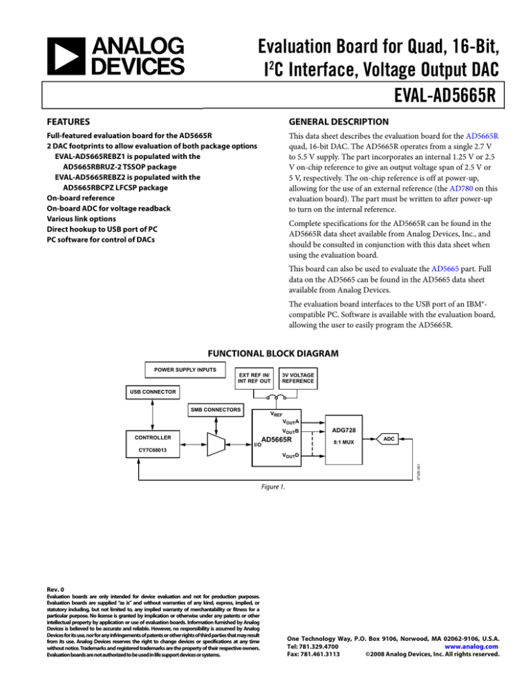
Evaluation Board for Quad, 16-Bit, I2C Interface, Voltage Output DAC EVAL-AD5665R FEATURES GENERAL DESCRIPTION Full-featured evaluation board for the AD5665R 2 DAC footprints to allow evaluation of both package options EVAL-AD5665REBZ1 is populated with the AD5665RBRUZ-2 TSSOP package EVAL-AD5665REBZ2 is populated with the AD5665RBCPZ LFCSP package On-board reference On-board ADC for voltage readback Various link options Direct hookup to USB port of PC PC software for control of DACs This data sheet describes the evaluation board for the AD5665R quad, 16-bit DAC. The AD5665R operates from a single 2.7 V to 5.5 V supply. The part incorporates an internal 1.25 V or 2.5 V on-chip reference to give an output voltage span of 2.5 V or 5 V, respectively. The on-chip reference is off at power-up, allowing for the use of an external reference (the AD780 on this evaluation board). The part must be written to after power-up to turn on the internal reference. Complete specifications for the AD5665R can be found in the AD5665R data sheet available from Analog Devices, Inc., and should be consulted in conjunction with this data sheet when using the evaluation board. This board can also be used to evaluate the AD5665 part. Full data on the AD5665 can be found in the AD5665 data sheet available from Analog Devices. The evaluation board interfaces to the USB port of an IBM®compatible PC. Software is available with the evaluation board, allowing the user to easily program the AD5665R. FUNCTIONAL BLOCK DIAGRAM POWER SUPPLY INPUTS EXT REF IN/ INT REF OUT 3V VOLTAGE REFERENCE USB CONNECTOR SMB CONNECTORS VREF VOUTA VOUTB CONTROLLER AD5665R I/O ADG728 8:1 MUX ADC CY7C68013 07305-001 VOUTD Figure 1. Rev. 0 Evaluation boards are only intended for device evaluation and not for production purposes. Evaluation boards are supplied “as is” and without warranties of any kind, express, implied, or statutory including, but not limited to, any implied warranty of merchantability or fitness for a particular purpose. No license is granted by implication or otherwise under any patents or other intellectual property by application or use of evaluation boards. Information furnished by Analog Devices is believed to be accurate and reliable. However, no responsibility is assumed by Analog Devices for its use, nor for any infringements of patents or other rights of third parties that may result from its use. Analog Devices reserves the right to change devices or specifications at any time without notice. Trademarks and registered trademarks are the property of their respective owners. Evaluation boards are not authorized to be used in life support devices or systems. One Technology Way, P.O. Box 9106, Norwood, MA 02062-9106, U.S.A. www.analog.com Tel: 781.329.4700 Fax: 781.461.3113 ©2008 Analog Devices, Inc. All rights reserved. EVAL-AD5665R TABLE OF CONTENTS Features .............................................................................................. 1 Installing the Software ..................................................................5 General Description ......................................................................... 1 Software Operation .......................................................................5 Functional Block Diagram .............................................................. 1 Evaluation Board Schematics and Artwork ...................................8 Revision History ............................................................................... 2 Ordering Information .................................................................... 12 Evaluation Board Hardware ............................................................ 3 Bill of Materials ........................................................................... 12 Power Supplies .............................................................................. 3 Ordering Guide .......................................................................... 12 Link Options ................................................................................. 3 ESD Caution................................................................................ 12 Evaluation Board Software .............................................................. 5 REVISION HISTORY 1/08—Revision 0: Initial Version Rev. 0 | Page 2 of 2 EVAL-AD5665R EVALUATION BOARD HARDWARE POWER SUPPLIES To power the EVAL-AD5665REBZ, supply the voltage (2.7 V to 5.5 V) between the AVDD and AGND inputs for the analog supply of the AD5665R (J6). Alternatively, placing Link 6 in Position B powers the analog circuitry from the USB port (default setting). This powers all devices with 3.3 V supply. Both AGND and DGND inputs are provided on the board. The AGND and DGND planes are connected at one location close to the AD5665R. To avoid ground loop problems, it is recommended not to connect AGND and DGND elsewhere in the system. Each supply is decoupled to the relevant ground plane with 10 μF and 0.1 μF capacitors. Each device supply pin is also decoupled with a 10 μF and 0.1 μF capacitor pair to the relevant ground plane. LINK OPTIONS A number of link and switch options on the evaluation board should be set for the required operating setup before using the board. The functions of these link options are described in detail in Table 2. The default setup is for control by the PC via the USB port and for evaluating the part in standard/fast mode with an external 3 V reference, the AD780. The default link options are listed in Table 1. Table 1. Link Options Setup for PC Control (Default) Link No. LK1 to LK4 LK5 LK6 LK7 LK8 LK9 LK10 LK11 LK12 LK13 LK14 LK15 LK16 Option Inserted B B A A A Removed B B A A A Inserted Table 2. Link Functions Link No. LK1 to LK4 LK5 LK6 LK7 LK8 LK9 LK10 LK11 LK12 Function These links connect the VOUTA to VOUTD pins of the AD5665R to the input pins of ADG728 demultiplexer to monitor the DAC output value using the on-board AD7992 ADC. This link selects the AVDD power supply source for the analog circuitry. Position A selects J6 as the AVDD analog circuitry power supply source. Position B selects the 3.3 V power supply source as the AVDD analog circuitry power supply source (see LK6). This link selects the DVDD supply source for the digital circuitry. Position A selects J7 as the digital circuitry power supply source. Position B selects the 3.3 V USB as the digital circuitry power supply source. This link selects whether the AD5665R evaluation board is controlled by the PC via the USB port or by an external source via the SMB connectors J1 to J12. Position A selects control by the PC via the USB port. Position B selects control by an external source via the SMB connectors J1 to J4. This link sets the RESET pin on the ADG728. Position A allows normal operation of the switch. Position B resets the switch. This link selects the AVDD power supply source for the AD780 reference. Position A selects J6-3 as the AD780 power supply source. Position B selects the 5 V USB supply voltage as the AD780 power supply source. This link connects a 0.1 μF capacitor to AGND on the VREFOUT pin. It is recommended to connect this when using the internal reference. This link selects the reference source. Position A selects the internal reference as the reference source. The part must be written to via software to turn on the internal reference. Position B selects the on-board AD780 3 V reference as the reference source. This link selects whether the part power-on resets to zero-scale or midscale. Position A ensures that the part power-on resets to midscale. Position B ensures that the part power-on resets to zero-scale. Rev. 0 | Page 3 of 3 EVAL-AD5665R Link No. LK13 LK14 LK15 LK16 Function This link selects the DAC voltage source. Position A selects the AVDD analog circuitry power supply source. Position B selects the on-board AD780 3 V reference as the power supply source. This link allows the user to hardwire the ADDR1 pin to set the two LSBs (A1, A0) of the 7-bit address. 00011A1A0 (10-lead LFCSP); 001A3A2A1A0 (14-lead TSSOP). Position A connects the pin to AVDD; therefore, two LSBs are 00. Position B connects the pin to GND; therefore, two LSBs are 11. No connection; therefore, two LSBs are 10. This link allows the user to hardwire the ADDR2 pin to set the bits (A3, A2) of the 7- bit address. 001A3A2A1A0 (14-lead TSSOP only). Position A connects the pin to AVDD; therefore, two bits are 00. Position B connects the pin to GND; therefore, two bits are 11. No connection; therefore, two bits are 10. This link connects the OP_SEL pin of the AD780 reference to ground, selecting a 3 V output. Leaving no connect gives a 2.5 V output. Rev. 0 | Page 4 of 4 EVAL-AD5665R EVALUATION BOARD SOFTWARE INSTALLING THE SOFTWARE 3. The AD5665R evaluation kit includes self-installing software on CD-ROM. The software is compatible with Microsoft® Windows® 2000 and Windows XP. Select the part number of the device on the evaluation board and click OK. 4. The main window of AD5665R evaluation software opens, as shown in Figure 3. The data programmed into the 24-bit input shift register is displayed. You can select the command bits, the address bits, and the data bits by clicking the appropriate option button under each section. The software should be installed before connecting the evaluation board to the PC’s USB port. This ensures that the board is correctly recognized when connected to the PC. 1. Start the Windows operating system and insert the CD-ROM. 2. The installation software should launch automatically. If it does not, run the setup.exe file directly from the CD. 3. 4. 1. After installation from the CD-ROM is complete, power up the AD5665R evaluation board as described in the Power Supplies section. Connect the board to the PC’s USB port using the supplied cable. To select a command to program the part, click the appropriate option button under the Command Bits section. For example, to program all DAC outputs with full scale, click Write to and Update DAC channel n. 2. Next, click All DACs in the Address Bits section. 3. Once the software detects the evaluation board, proceed through any dialog boxes that appear to finalize the installation. Then, in the Data Bits section, enter the data in the Hex Value or Voltage box. 4. To execute, click Write to Part. You must click Write to Part to execute all writes to the part. SOFTWARE OPERATION 2. From the Analog Devices menu, click Start > All Programs > Analog Devices > AD5665R > AD5665R Evaluation Software. The AD5665R evaluation software also allows programming of the power-down DAC bits, the clear code register bits, and the LDAC register bits by clicking the corresponding option button under the Command Bits section and then clicking Write to Part. You can also set the register bits for the required mode of operation. Consult the AD5665R data sheet for details. For older PCs, click Start > Programs > Analog Devices > AD5665R > AD5665R Evaluation Software. ADC The device selection window opens, as shown in Figure 2. The voltage output on each DAC channel is monitored using the on-board ADC. To read the output voltage, click the Sample button in the ADC section (upper right portion of the window). 07305-002 1. Command Bits Figure 2. Device Selection Window Rev. 0 | Page 5 of 5 07305-003 EVAL-AD5665R Figure 3. AD5665R Evaluation Software Main Window Rev. 0 | Page 6 of 6 EVAL-AD5665R Reference Setup 07305-004 The AD5665R internal reference is turned off at power-up by default, allowing the use of an external reference. To turn on (or turn off) the internal reference, click Internal Reference Setup in the Command Bits section. This allows you to program the bit in the reference setup register for the required mode of operation, as shown in Figure 4. Then click Write to Part. Figure 4. AD5665R Evaluation Software Main Window, Reference Setup Rev. 0 | Page 7 of 7 EVAL-AD5665R EVALUATION BOARD SCHEMATICS AND ARTWORK 07305-005 Figure 5. Schematic of Controller Circuitry Rev. 0 | Page 8 of 8 EVAL-AD5665R 07305-006 Figure 6. Schematic of AD5665R Circuitry Rev. 0 | Page 9 of 9 07305-007 EVAL-AD5665R 07305-008 Figure 7. Component Placement Drawing Figure 8. Component Side PCB Drawing Rev. 0 | Page 10 of 10 07305-009 EVAL-AD5665R Figure 9. Solder Side PCB Drawing Rev. 0 | Page 11 of 11 EVAL-AD5665R ORDERING INFORMATION BILL OF MATERIALS Table 3. Qty 1 1 1 1 1 1 1 1 1 1 9 1 1 1 1 1 5 1 2 24 1 2 4 1 4 1 2 2 1 1 6 10 19 Reference Designator U1 U2 U4 U5 U6 U7 U8 U9 U10 Y1 VOUTA to VOUTD; J1 to J3, J11, J12 J10 J6 J7 D1 L1 C1, C4, C5, C18, C35 C11 C26, C27 C2, C3, C6 ,C7, C8, C9, C12, ,C17, C19 to C23, C25, C28 to C34, C36, C37, C39 C24 C10, C38 C13 to C16 R1 R2 to R5 R6 R7, R8 R11, R12 R10 R9 LK1 to LK4, LK10, LK16 LK5 to LK9, LK11 to LK15 T1 to T4, T7 to T21 Description AD5665RBRUZ-2 ADG774BRQ AD780ARZ AD7992BRMZ-1 ADG728BRU ADP3303AR-3.3 CY7C68013-CSP 24LC01 AD5665RBCPZ 24 MHz crystal Gold 50 Ω SMB jack USB Mini B Power connectors Power connectors LED Bead 10 μF 10 V tantalum capacitor (TAJ-B package) 1 μF 10 V tantalum capacitor (TAJ-B package) 22 pF (0603 package) 0.1 μF (0603 package) Supplier/Number Analog Devices Analog Devices Analog Devices Analog Devices Analog Devices Analog Devices Embassy CY7C68013-56LFC FEC 975-8070 Analog Devices FEC 569-872 FEC 1019324 FEC 476-8309 FEC 963-3972 FEC 963-2980 FEC 515-620 FEC 9526862 FEC 197-130 FEC 1135234 FEC 722-005 FEC 9632972 2.2 μF (0603 package) 1 μF (0603 package) 0805 package (not inserted) 1.5 Ω Wire-wrap pin (not inserted) 1 kΩ (0603 package) 100 kΩ (0603 package) 2.2 kΩ(0603 package) 10 kΩ (0603 package) 0 Ω (0603 package) Header (2 × 1 pin) Header (3 × 1 pin) Test point FEC 9632972 FEC 9632972 ORDERING GUIDE Model EVAL-AD5665REBZ1 1 EVAL-AD5665REBZ21 1 ESD CAUTION Description TSSOP Evaluation Board, Populated with AD5665RBRUZ-2 LFCSP Evaluation Board, Populated with AD5665RBCPZ Z = RoHS Compliant Part. ©2008 Analog Devices, Inc. All rights reserved. Trademarks and registered trademarks are the property of their respective owners. EB07305-0-1/08(0) Rev. 0 | Page 12 of 12 FEC 758-267 FEC 911-239 FEC 911 471 FEC 911-276 FEC 911-355 FEC 772-227 FEC 511-705 FEC 511-717 FEC 873-1144
