Dual-Channel CCD Signal Processor with Precision Timing ADDI7013 Data Sheet
advertisement

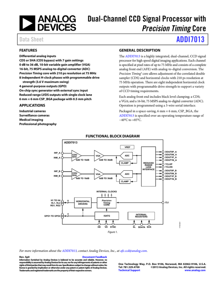
Dual-Channel CCD Signal Processor with Precision Timing Core ADDI7013 Data Sheet FEATURES GENERAL DESCRIPTION Differential analog inputs CDS or SHA (CDS bypass) with 7 gain settings 0 dB to 36 dB, 10-bit variable gain amplifier (VGA) 16-bit, 75 MSPS analog-to-digital converter (ADC) Precision Timing core with 210 ps resolution at 75 MHz 8 independent H-clock phases with programmable drive strength (3.6 V maximum swing) 4 general-purpose outputs (GPO) On-chip sync generator with external sync input Reduced range LVDS outputs with single clock lane 6 mm × 6 mm CSP_BGA package with 0.5 mm pitch The ADDI7013 is a highly integrated, dual-channel, CCD signal processor for high speed digital imaging applications. Each channel is specified at pixel rates of up to 75 MHz and consists of a complete analog front end (AFE) with analog-to-digital conversion. The Precision Timing® core allows adjustment of the correlated double sampler (CDS) and horizontal clocks with 210 ps resolution at 75 MHz operation. There are eight independent horizontal clock outputs with programmable drive strength to support a variety of CCD timing requirements. Each analog front end includes black level clamping; a CDS; a VGA; and a 16-bit, 75 MSPS analog-to-digital converter (ADC). Operation is programmed using a 3-wire serial interface. APPLICATIONS Packaged in a space-saving, 6 mm × 6 mm, CSP_BGA, the ADDI7013 is specified over an operating temperature range of −40°C to +85°C. Industrial cameras Surveillance cameras Medical imaging Professional photography FUNCTIONAL BLOCK DIAGRAM ADDI7013 VREF INP_A CDS/ SHA 0dB TO 18dB INM_A DOUT0P_A DOUT0N_A DOUT1P_A DOUT1N_A ADC VGA 0dB TO 36dB REDUCED RANGE LVDS INTERFACE CLAMP INP_B CDS/ SHA 0dB TO 18dB INM_B ADC VGA 0dB TO 36dB TCLKP TCLKN DOUT0P_B DOUT0N_B DOUT1P_B DOUT1N_B CLAMP INTERNAL CLOCKS 8 Precision Timing CORE HORIZONTAL DRIVERS 4 INTERNAL REGISTERS ISATG GPO1 TO GPO4 HD VD CLI SYNC SL SDATA SCK 11784-001 H1 TO H4 HL1, HL2 RG1, RG2 Figure 1. For more information about the ADDI7013, contact Analog Devices, Inc., at afe.ccd@analog.com. Rev. Sp0 Document Feedback Information furnished by Analog Devices is believed to be accurate and reliable. However, no responsibility is assumed by Analog Devices for its use, nor for any infringements of patents or other rights of third parties that may result from its use. Specifications subject to change without notice. No license is granted by implication or otherwise under any patent or patent rights of Analog Devices. Trademarks and registered trademarks are the property of their respective owners. One Technology Way, P.O. Box 9106, Norwood, MA 02062-9106, U.S.A. Tel: 781.329.4700 ©2013 Analog Devices, Inc. All rights reserved. Technical Support www.analog.com ADDI7013 Data Sheet NOTES ©2013 Analog Devices, Inc. All rights reserved. Trademarks and registered trademarks are the property of their respective owners. D11784F-0-10/13(Sp0) Rev. Sp0 | Page 2 of 2

