MT-077 TUTORIAL Log Amp Basics
advertisement

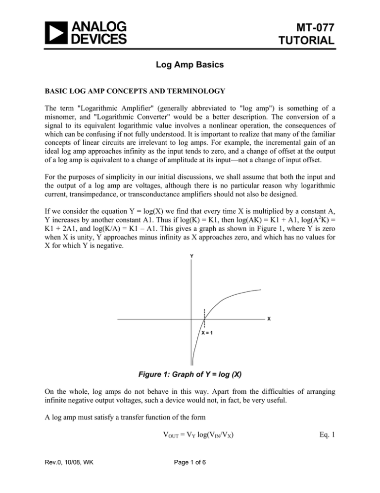
MT-077 TUTORIAL Log Amp Basics BASIC LOG AMP CONCEPTS AND TERMINOLOGY The term "Logarithmic Amplifier" (generally abbreviated to "log amp") is something of a misnomer, and "Logarithmic Converter" would be a better description. The conversion of a signal to its equivalent logarithmic value involves a nonlinear operation, the consequences of which can be confusing if not fully understood. It is important to realize that many of the familiar concepts of linear circuits are irrelevant to log amps. For example, the incremental gain of an ideal log amp approaches infinity as the input tends to zero, and a change of offset at the output of a log amp is equivalent to a change of amplitude at its input—not a change of input offset. For the purposes of simplicity in our initial discussions, we shall assume that both the input and the output of a log amp are voltages, although there is no particular reason why logarithmic current, transimpedance, or transconductance amplifiers should not also be designed. If we consider the equation Y = log(X) we find that every time X is multiplied by a constant A, Y increases by another constant A1. Thus if log(K) = K1, then log(AK) = K1 + A1, log(A2K) = K1 + 2A1, and log(K/A) = K1 – A1. This gives a graph as shown in Figure 1, where Y is zero when X is unity, Y approaches minus infinity as X approaches zero, and which has no values for X for which Y is negative. Y X X=1 Figure 1: Graph of Y = log (X) On the whole, log amps do not behave in this way. Apart from the difficulties of arranging infinite negative output voltages, such a device would not, in fact, be very useful. A log amp must satisfy a transfer function of the form VOUT = VY log(VIN/VX) Rev.0, 10/08, WK Page 1 of 6 Eq. 1 MT-077 over some range of input values which may vary from 100:1 (40 dB) to over 1,000,000:1 (120 dB). With inputs very close to zero, log amps cease to behave logarithmically, and most then have a linear VIN/VOUT law. This behavior is often lost in device noise. Noise often limits the dynamic range of a log amp. The constant, VY, has the dimensions of voltage, because the output is a voltage. The input, VIN, is divided by a voltage, VX, because the argument of a logarithm must be a simple dimensionless ratio. A graph of the transfer characteristic of a log amp is shown in Figure 2. The scale of the horizontal axis (the input) is logarithmic, and the ideal transfer characteristic is a straight line. When VIN = VX, the logarithm is zero (log 1 = 0). VX is therefore known as the intercept voltage of the log amp because the graph crosses the horizontal axis at this value of VIN. VYLOG (VIN/VX) IDEAL ACTUAL 2VY SLOPE = VY VY VOUT = VY log10 VIN VX + 0 ACTUAL - IDEAL VIN=VX VIN=10VX VIN=100VX INPUT ON LOG SCALE Figure 2: Log Amp Transfer Function The slope of the line is proportional to VY. When setting scales, logarithms to the base 10 are most often used because this simplifies the relationship to decibel values: when VIN = 10VX, the logarithm has the value of 1, so the output voltage is VY. When VIN = 100VX, the output is 2VY, and so forth. VY can therefore be viewed either as the "slope voltage" or as the "volts per decade factor." The logarithm function is indeterminate for negative values of x. Log amps can respond to negative inputs in three different ways: (1) They can give a fullscale negative output as shown in Figure 3. (2) They can give an output which is proportional to the log of the absolute value of the input and disregards its sign as shown in Figure 4. This type of log amp can be considered to be a full-wave detector with a logarithmic characteristic, and is often referred to as a detecting log amp. (3) They can give an output which is proportional to the log of the absolute value of the input and has the same sign as the input as shown in Figure 5. This type of log amp can be considered to be a video amp with a logarithmic characteristic, and may be known as a logarithmic video (log video) amplifier or, sometimes, a true log amp. Page 2 of 6 MT-077 + OUTPUT + - INPUT - Figure 3: Basic Log Amp (Saturates with Negative Input) + OUTPUT + - INPUT - Figure 4: Detecting Log Amp (Output Polarity Independent of Input Polarity) + OUTPUT + - INPUT - Figure 5: Log Video or “True Log Amp” (Symmetrical Response to Positive or Negative Signals) Page 3 of 6 MT-077 LOG AMP ARCHITECTURES There are three basic architectures which may be used to produce log amps: the basic diode log amp, the successive detection log amp, and the "true log amp" which is based on cascaded semilimiting amplifiers. The voltage across a silicon diode is proportional to the logarithm of the current through it. If a diode is placed in the feedback path of an inverting op-amp, the output voltage will be proportional to the log of the input current as shown in Figure 6. V= + V- kT In q I IO -VIN ( ) I = IIN RIN IIN if I >> IO + - EO I EO = V kT ln q ( IIO)≅ 0.06 log RVININIO if I >> IO Figure 6: The Diode / Op-Amp Log Amp In practice, the dynamic range of this configuration is limited to 40-60 dB because of non-ideal diode characteristic, but if the diode is replaced with a diode-connected transistor as shown in Figure 7, the dynamic range can be extended to 120 dB or more. IC IE + EO IIN - EO = IIN kT ln I q ES Figure 7: Transistor / Op-Amp Log Amp Page 4 of 6 MT-077 This type of log amp has three disadvantages: (1) both the slope and intercept are temperature dependent; (2) it will only handle unipolar signals; and (3) its bandwidth is both limited and dependent on signal amplitude. Where several such log amps are used on a single chip to produce an analog computer which performs both log and antilog operations, the temperature variation in the log operations is unimportant, since it is compensated by a similar variation in the antilogging. This makes possible the AD538, a monolithic analog computer which can multiply, divide, and raise to powers (see Figure 8). Where actual logging is required, however, the AD538 and similar circuits require temperature compensation. The major disadvantage of this type of log amp for high frequency applications, though, is its limited frequency response—which cannot be overcome. However carefully the amplifier is designed, there will always be a residual feedback capacitance CC (often known as Miller capacitance), from output to input which limits the high frequency response (See Figure 7). Figure 8: AD538 Log Amp Simplified Diagram What makes this Miller capacitance particularly troublesome is that the impedance of the emitter-base junction is inversely proportional to the current flowing in it—so that if the log amp has a dynamic range of 1,000,000:1, then its bandwidth will also vary by 1,000,000:1. In practice, the variation is less because other considerations limit the large signal bandwidth, but it is very difficult to make a log amp of this type with a small-signal bandwidth greater than a few hundred kHz. Log amps suitable for high frequency operation are discussed in Tutorial MT-078. Page 5 of 6 MT-077 REFERENCES 1. Hank Zumbahlen, Basic Linear Design, Analog Devices, 2006, ISBN: 0-915550-28-1. Also available as Linear Circuit Design Handbook, Elsevier-Newnes, 2008, ISBN-10: 0750687037, ISBN-13: 9780750687034. Chapter 2, 4. Copyright 2009, Analog Devices, Inc. All rights reserved. Analog Devices assumes no responsibility for customer product design or the use or application of customers’ products or for any infringements of patents or rights of others which may result from Analog Devices assistance. All trademarks and logos are property of their respective holders. Information furnished by Analog Devices applications and development tools engineers is believed to be accurate and reliable, however no responsibility is assumed by Analog Devices regarding technical accuracy and topicality of the content provided in Analog Devices Tutorials. Page 6 of 6


