MT-063 TUTORIAL Basic Three Op Amp In-Amp Configuration
advertisement
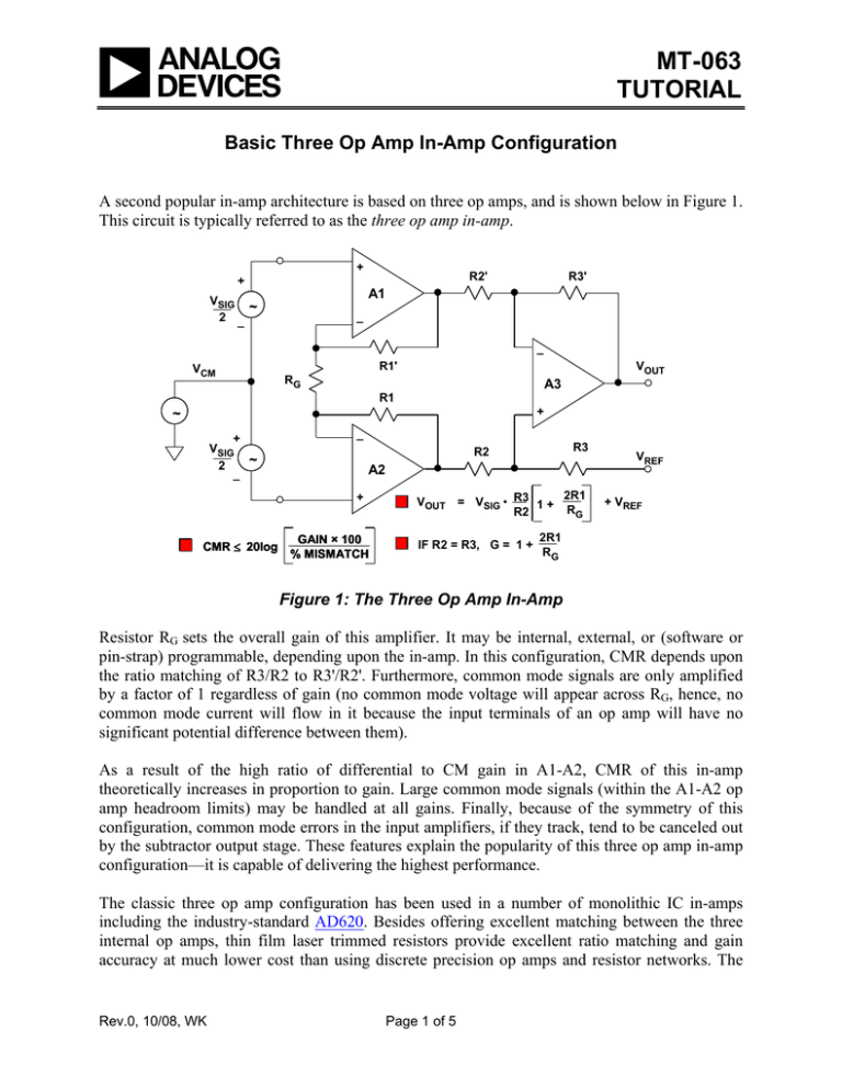
MT-063 TUTORIAL Basic Three Op Amp In-Amp Configuration A second popular in-amp architecture is based on three op amps, and is shown below in Figure 1. This circuit is typically referred to as the three op amp in-amp. + R2' + R3' A1 VSIG ~ 2 _ _ _ VCM R1' VOUT RG A3 R1 + ~ + VSIG ~ 2 _ _ A2 + CMR ≤ 20log R3 R2 GAIN × 100 % MISMATCH 2R1 VOUT = VSIG • R3 1 + RG R2 IF R2 = R3, G = 1 + VREF + VREF 2R1 RG Figure 1: The Three Op Amp In-Amp Resistor RG sets the overall gain of this amplifier. It may be internal, external, or (software or pin-strap) programmable, depending upon the in-amp. In this configuration, CMR depends upon the ratio matching of R3/R2 to R3'/R2'. Furthermore, common mode signals are only amplified by a factor of 1 regardless of gain (no common mode voltage will appear across RG, hence, no common mode current will flow in it because the input terminals of an op amp will have no significant potential difference between them). As a result of the high ratio of differential to CM gain in A1-A2, CMR of this in-amp theoretically increases in proportion to gain. Large common mode signals (within the A1-A2 op amp headroom limits) may be handled at all gains. Finally, because of the symmetry of this configuration, common mode errors in the input amplifiers, if they track, tend to be canceled out by the subtractor output stage. These features explain the popularity of this three op amp in-amp configuration—it is capable of delivering the highest performance. The classic three op amp configuration has been used in a number of monolithic IC in-amps including the industry-standard AD620. Besides offering excellent matching between the three internal op amps, thin film laser trimmed resistors provide excellent ratio matching and gain accuracy at much lower cost than using discrete precision op amps and resistor networks. The Rev.0, 10/08, WK Page 1 of 5 MT-063 AD620 is an excellent example of monolithic IC in-amp technology. A simplified device schematic is shown in Figure 2 below. +VS 49.4kΩ RG = G – 1 VB _ + _ + A1 A2 10kΩ 10kΩ _ 10kΩ A3 + VO 10kΩ Q1 400Ω 24.7kΩ 24.7kΩ Q2 VREF 400Ω RG –IN +IN –VS Figure 2: The AD620 In-Amp Simplified Schematic The AD620 is a highly popular in-amp and is specified for power supply voltages from ±2.3 V to ±18 V. Input voltage noise is only 9 nV/√Hz @ 1 kHz. Maximum input bias current is only 1 nA, due to the use of superbeta transistors for Q1-Q2. Overvoltage protection is provided by the internal 400Ω thin-film current-limit resistors in conjunction with the diodes connected from the emitter-to-base of Q1 and Q2. The gain G is set with a single external RG resistor, as noted by Equation 1 below. G = (49.4kΩ/RG) + 1 Eq. 1 As can be noted from this expression and Fig. 2, the AD620 internal resistors are trimmed so that standard 1% or 0.1% resistors can be used to set gain to popular values. As is true in the case of the two op amp in-amp configuration, single supply operation of the three op amp in-amp requires an understanding of the internal node voltages. Figure 3 below shows a generalized diagram of the in-amp operating on a single +5V supply. The maximum and minimum allowable output voltages of the individual op amps are designated VOH (maximum high output) and VOL (minimum low output) respectively. Note that the gain from the common mode voltage to the outputs of A1 and A2 is unity. It can be stated that the sum of the common mode voltage and the signal voltage at these outputs must fall within the amplifier output voltage range. Obviously this configuration cannot handle input Page 2 of 5 MT-063 common mode voltages of either zero volts or +5 V, because of saturation of A1 and A2. As in the case of the two op amp in-amp, the output reference is positioned halfway between VOH and VOL to allow for bipolar differential input signals. VCM + + R2' + _ R1' VOH=4.9V VOL=0.1V _ VOUT RG A3 R1 ~ VOH=4.9V VOL=0.1V + _ + VSIG 2 R2' A1 VSIG ~ 2 _ VCM GVSIG 2 R2 ~ VOH=4.9V VOL=0.1V VOUT = GVSIG + VREF R2 A2 _ VREF = 2.5V + 2R1 G = 1+ RG VCM – GVSIG 2 Figure 3: Three Op Amp In-Amp Single +5V Supply Restrictions While there are a number of good single-supply in-amps, the highest performance devices are still among those specified for traditional dual-supply operation, i.e., the just-discussed AD620 or the more recently introduced AD8221 and AD8222. For certain applications, even such devices as the AD620, which has been designed for dual supply operation, can be used with full precision on a single-supply power system. THE AD623 SINGLE-SUPPLY IN-AMP Like the two op amp in-amp counterparts discussed previously, three op amp in-amps require special design attention for wide CM range inputs on single power supplies. The AD623 single supply in-amp configuration, shown below in Figure 4 offers an attractive solution. In this device PNP emitter follower level shifters Q1 and Q2 allow the input signal to go 150 mV below the negative supply, and to within 1.5 V of the positive supply. The AD623 is fully specified for both single power supplies between +3 V and +12 V, and dual supplies between ±2.5 V and ±6 V. Page 3 of 5 MT-063 +VS + 50kΩ 50kΩ A1 –IN Q1 _ 50kΩ _ –VS A3 RG VOUT 50kΩ +VS + _ 50kΩ 50kΩ A2 +IN VREF + Q2 –VS Figure 4: AD623 Single-Supply In-Amp Architecture The AD623 data sheet contains excellent discussions and data on allowable input/output voltage ranges as a function of gain and power supply voltages. In addition, interactive design tools are available on the ADI web site which perform gain and range calculations relating these parameters for a number of in-amps, including the AD623. The key specifications of the AD623 are summarized in Figure 5. Wide Supply Range: +3V to ±6V Input Voltage Range: –VS – 0.15V to +VS – 1.5V 575µA Maximum Supply Current Gain Range: 1 to 1000 100µV Maximum Input Offset Voltage (AD623B) 1µV/°C Maximum Offset Voltage TC (AD623B) 50ppm Gain Nonlinearity 105dB CMR @ 60Hz, 1kΩ Source Imbalance, G ≥ 100 3µV p-p 0.1Hz to 10Hz Input Voltage Noise (G = 1) Figure 5: AD623 In-Amp Key Specifications Page 4 of 5 MT-063 The AD8223 is an integrated single-supply instrumentation amplifier that delivers rail-to-rail output swing on a single supply (+3.0 V to +25 V supplies). The input common-mode voltage includes the negative supply rail. The AD8223 offers superior user flexibility by allowing singlegain set resistor programming, and conforming to the 8-lead industry standard pinout configuration. With no external resistor, the AD8223 is configured for G = 5 and with an external resistor, the AD8223 can be programmed for gains up to 1000. The AD8223 utilizes the three op amp architecture described in this tutorial. REFERENCES 1. Hank Zumbahlen, Basic Linear Design, Analog Devices, 2006, ISBN: 0-915550-28-1. Also available as Linear Circuit Design Handbook, Elsevier-Newnes, 2008, ISBN-10: 0750687037, ISBN-13: 9780750687034. Chapter 2. 2. Walter G. Jung, Op Amp Applications, Analog Devices, 2002, ISBN 0-916550-26-5, Also available as Op Amp Applications Handbook, Elsevier/Newnes, 2005, ISBN 0-7506-7844-5. Chapter 2. 3. Charles Kitchin and Lew Counts, A Designer's Guide to Instrumentation Amplifiers, 3rd Edition, Analog Devices, 2006. Copyright 2009, Analog Devices, Inc. All rights reserved. Analog Devices assumes no responsibility for customer product design or the use or application of customers’ products or for any infringements of patents or rights of others which may result from Analog Devices assistance. All trademarks and logos are property of their respective holders. Information furnished by Analog Devices applications and development tools engineers is believed to be accurate and reliable, however no responsibility is assumed by Analog Devices regarding technical accuracy and topicality of the content provided in Analog Devices Tutorials. Page 5 of 5

