a AN-410 APPLICATION NOTE •
advertisement
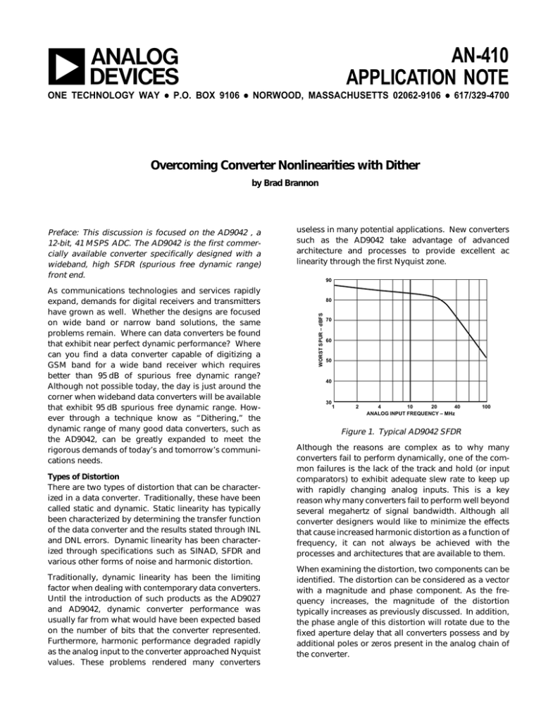
a ONE TECHNOLOGY WAY • P.O. AN-410 APPLICATION NOTE BOX 9106 • NORWOOD, MASSACHUSETTS 02062-9106 • 617/329-4700 Overcoming Converter Nonlinearities with Dither by Brad Brannon As communications technologies and services rapidly expand, demands for digital receivers and transmitters have grown as well. Whether the designs are focused on wide band or narrow band solutions, the same problems remain. Where can data converters be found that exhibit near perfect dynamic performance? Where can you find a data converter capable of digitizing a GSM band for a wide band receiver which requires better than 95 dB of spurious free dynamic range? Although not possible today, the day is just around the corner when wideband data converters will be available that exhibit 95 dB spurious free dynamic range. However through a technique know as “Dithering,” the dynamic range of many good data converters, such as the AD9042, can be greatly expanded to meet the rigorous demands of today’s and tomorrow’s communications needs. Types of Distortion There are two types of distortion that can be characterized in a data converter. Traditionally, these have been called static and dynamic. Static linearity has typically been characterized by determining the transfer function of the data converter and the results stated through INL and DNL errors. Dynamic linearity has been characterized through specifications such as SINAD, SFDR and various other forms of noise and harmonic distortion. Traditionally, dynamic linearity has been the limiting factor when dealing with contemporary data converters. Until the introduction of such products as the AD9027 and AD9042, dynamic converter performance was usually far from what would have been expected based on the number of bits that the converter represented. Furthermore, harmonic performance degraded rapidly as the analog input to the converter approached Nyquist values. These problems rendered many converters useless in many potential applications. New converters such as the AD9042 take advantage of advanced architecture and processes to provide excellent ac linearity through the first Nyquist zone. 90 80 WORST SPUR – dBFS Preface: This discussion is focused on the AD9042 , a 12-bit, 41 MSPS ADC. The AD9042 is the first commercially available converter specifically designed with a wideband, high SFDR (spurious free dynamic range) front end. 70 60 50 40 30 1 2 10 4 20 40 ANALOG INPUT FREQUENCY – MHz 100 Figure 1. Typical AD9042 SFDR Although the reasons are complex as to why many converters fail to perform dynamically, one of the common failures is the lack of the track and hold (or input comparators) to exhibit adequate slew rate to keep up with rapidly changing analog inputs. This is a key reason why many converters fail to perform well beyond several megahertz of signal bandwidth. Although all converter designers would like to minimize the effects that cause increased harmonic distortion as a function of frequency, it can not always be achieved with the processes and architectures that are available to them. When examining the distortion, two components can be identified. The distortion can be considered as a vector with a magnitude and phase component. As the frequency increases, the magnitude of the distortion typically increases as previously discussed. In addition, the phase angle of this distortion will rotate due to the fixed aperture delay that all converters possess and by additional poles or zeros present in the analog chain of the converter. menon is frequently observed as fluctuations in the SFDR of a converter as the input frequency is swept through the input bandwidth. FREQUENCY 3 FREQUENCY 2 FREQUENCY 1 FREQUENCY 2 NET 0 Figure 2. ALL FREQUENCIES Static linearity is usually stated in terms of the dc transfer function. There are many methods that can be used to capture the transfer function of a given data converter. Traditional evaluation of this function includes specifications such as Integral Nonlinearity (INL) and Differential Nonlinearity (DNL) errors. However, stating that a converter has an INL error of 3/4 LSB and a DNL of 0.5 LSB is not very descriptive of the device unless it is to be used as a digitizer in a sampling application such as a CCD digitizer or sampling scope. In communications applications, the static linearity results reported in a typical data sheet are all but meaningless. This is not to say that the static transfer function is unimportant. On the contrary, the static transfer function of the data converters does determine dynamic performance, and as such, some analysis of how the static transfer function behaves is worth discussion. Additionally, as designers have focused on improving the characteristics of internal track-and-holds, SFDR has become limited, not by analog slew rate but DNL errors in the transfer function. Figure 4. High performance converters such as the AD9042 have static transfer functions that do not change as a function of frequency, and additionally the distortion due to slew limited effects is typically much better than 80 dB as shown in Figure 1. This is especially true when the analog input is away from full scale. Since many communications applications both wide and narrow band frequently operate with signals well below full scale, this is an important region to examine in high performance converters. Dynamic Effects of Static Linearity As stated earlier, INL and DNL reports alone are not sufficient to characterize a converter’s performance for communications applications. For example, a converter may have a worst case DNL of +2 LSB, 1 code from –FS. Although this is quite a bad error, its effect on a converter in a receiver application will be minimal since the converter rarely uses codes near ± full scale. Conversely, a converter may have a worst DNL error of +0.25, near midscale. After careful examination, it is revealed that there is a series of four codes together, each of them +0.25 LSB. The net effect on the converter is a transfer function error of +1 LSB at that location, a rather significant error. As shown in Figure 5, a signal that never reaches full scale may never hit the bad codes unless the converter is clipped anyway. Likewise, a converter with four typical errors in the middle of the range will be repetitively exercised causing potential dynamic troubles. Thus a blanket statement about the INL or DNL of a converter without additional information (location, frequency, etc.) is almost useless. If the transfer function of the data converter is used to fit an ideal sinusoidal signal, a spectral analysis can be performed on the resulting data to determine how these static characteristic of the device affect SFDR. These results will show the magnitude and phase of the harmonic distortion and can easily be swept over amplitude. Since the static transfer function is not frequency dependent in high performance converters like the AD9042, the distortion vector is constant for all frequencies as shown below, although each harmonic 2 through n has a different set of vectors. DNL PLOT 2 LSBs ERROR BAD CODE +2 LSBs ALL FREQUENCIES 1 4 BAD CODES WITH DNL OF +0.25 PERFECT DNL 0 –1 –2 Figure 3. 0 4095 % OCCURRENCE PROBABILITY OF CODE OCCURRENCE FOR A SINE INPUT Since the distortion is now defined in terms of vectors, the static and dynamic performance of a data converter can be summed together. In fact, it is possible for the terms to exactly cancel out as shown below, causing such a converter to have better mid-band performance than at either lower or higher frequency. This pheno- 3 –30 dB CUSP FULL SCALE CUSP 0 4095 0 Figure 5. –2– +DNL: 0.16 AT 959 +DNL: 0.36 AT 3967 –DNL: –0.43 AT 1041 –DNL: –0.22 AT 2784 +INL: 0.66 AT 2586 +INL: 0.41 AT 3230 –INL: –0.44 AT 4082 –INL: –0.56 AT 3882 b. a. Figure 6. By using this equation with a full-scale signal, it is shown that the probability of a full-scale code occurring is 1 percent for a 12-bit converter. In contrast, the probability of a midscale code occurring is only 0.015 percent, defining the typical “cusp” associated with the PDF of a sine wave. This is due to the fact that the slew rate of the sine function is greatest at midscale and zero at the max/ min. Therefore, on a per sample basis, the likelihood of sampling the signal at the max/min is greater that at the zero crossing. In fact, if the PDF array is multiplied by the DNL error array and integrated, the resultant is the total error that could be expected for a full-scale sine wave with the given DNL error. High resolution data converters typically use multistage techniques to achieve high bit resolution without large comparator arrays that would be required if traditional “flash” ADC techniques were employed. The multistage converter typically provides more economic use of silicon. However, since it is a multistage device, certain portions of the circuit are used repetitively as the analog input sweeps from one end of the converter to the other, as shown in Figure 6. Although the worst DNL error may be less than 0.25 LSB, the repetitive nature of the transfer function can play havoc with low level dynamic signals. Full-scale SFDR may be 88 dBFS, however 20 dB below full scale, these repetitive DNL errors may cause SFDR to fall to 80 dBFS. max code Error total = The plots above were taken from two different AD9042s. Although each is quite good, both the INL and DNL plot pairs above show dramatically different linearity characteristics. Both clearly show the repetitive nature of linearity in multistage converters. What about the case where the input signal is –30 dB below full scale? In this case, only just over 3 percent of the converter codes are exercised. In this example, the codes at the peak of the sine wave now have a probability of occurring of 3 percent, and midscale codes 0.5 percent. As before, if the PDF array for the reduced amplitude sine is multiplied by the DNL errors for those same codes and integrated, then the resultant is the total error that could be expected for the reduced amplitude signal. If the process is again performed at a signal at –60 dB below full scale, only 0.1 percent (4 codes) are exercised. For this case the peak codes occur about 28 percent, and the middle codes 22 percent. As before, if the PDF array is multiplied by the DNL error array and integrated, the overall error would result. Probability To begin to understand how DNL can possibly affect the dynamic performance of a data converter, it is necessary to examine the probability density function (PDF) of a sinusoidal function stimulating the data converter. The equation below expresses the probability of any converter code occurring. P( I th code) = ( N −1 1 −1 V I − 2 sin π A2 N ) − sin ( ) V I −1 − 2 N −1 A2 N −1 ∫ P(I ) × DNL(I ) I =min code V is the full-scale range of the converter. N is the number of bits in the converter. How does this relate to dynamic performance? Assume for example that all converter codes exhibit perfect DNL (i.e., 0 error) except for code number 1985 which has a DNL error of +1.5 LSB. With a full-scale sinusoidal input, I is the code in question. A is the peak amplitude of the input sine wave. –3– the additional error (besides normal quantization error) is 1.5 × 0.0001555 or 0.00023325 LSBs. However, with a signal at –30 dB below full scale, the equation is now 1.5 × 0.03 or 0.045 LSBs, and the contribution is now almost 200 times greater at the reduced signal level than when the input was at full scale. Furthermore, since the shape of the PDF is a cusp as shown in Figure 7, it can be expected that dynamic performance can be predicted to gradually worsen as the rim of the cusp approaches code 1985, then quickly return to near perfect performance when the signal falls below –30 dB where code 1985 is no longer exercised. The Nature of DNL To understand the nature of DNL in any converter, it is necessary to understand the architecture of the converter in question. The diagram shown in Figure 8 is that of the AD9042, a 12-bit, 41 MSPS analog-to-digital converter. As stated above, nearly all high resolution converters such as the AD9042 employ some form of multistage conversion. In the AD9042, the first converter is a 6-bit ADC. The second converter is a 7-bit converter. The combined total is 12 data bits plus 1 error correction bit to internally compensate for nonlinearities of the 6bit ADC. For any multistage converter to properly operate, a highly accurate digital-to-analog converter must be employed to convert the first stage ADC (6 bits in the AD9042) back into analog for subtraction from the original input. In the AD9042, this DAC is nearly 14 bits accurate. Following the DAC in the architecture is an amplifier that is used to perform the subtraction and gain ranging for the second ADC (7 bits in the AD9042). Again, the gain of the amplifier must be matched precisely to the range of the second ADC. If any of these conditions are not exactly met, the result will be mismatches that show up as DNL errors, much worse than those shown in the actual DNL plots. Not a lot of gain mismatch is required to cause problems. For example, even if matching is maintained to 12 bits, the DNL error generated could be ± 1 LSB. Even if 14-bit matching is achieved, the overall DNL errors will be ±0.25 LSB as in the AD9042. Thus from the actual DNL plots shown earlier, it is apparent that matching is maintained between 13 and 14 bits despite the fact that the AD9042 is an untrimmed device. In this example, since the error only occurs only at the signal peak with the reduced signal, the primary contributor as the signal is reduced is the second harmonic. In a practical converter, the DNL errors are complex and frequently repetitive as shown in the figures of the previous sections. It is this effect that dither seeks to remove in order to improve (or maintain) as the signal levels are reduced. DNL PLOT 2 LSBs ERROR BAD CODE 1985 DNL +1.5 1 PERFECT DNL 0 –1 –2 % OCCURRENCE % OCCURRENCE 0 2 90 4095 PROBABILITY OF CODE OCCURRENCE –30 dB CUSP FULL SCALE CUSP 0 0 4095 Furthermore, in a multistage converter, since the range of the second stage ADC is used over many times, the DNL pattern will repeat many times. In fact, the DNL repeat count will be 2N where N is the number of bits in the first ADC. In the AD9042, N is equal to 6 and the repeat count is therefore 64. By careful observation of the actual DNL plots above, it is observed that the DNL spikes occur 64 times. This logic is valid for any multistage converter as well as some “Flash” ADCs that may have segmented resistive ladders. 86 82 78 74 70 –35 –30 –25 –20 –15 –10 SIGNAL LEVEL – dBFS –5 0 Figure 7. Signal Level AVCC DVCC AIN A1 TH1 TH2 TH3 A2 ADC VOFFSET VREF +2.4V REFERENCE ADC 7 DAC AD9042 6 ENCODE ENCODE INTERNAL TIMING DIGITAL ERROR CORRECTION LOGIC (MSB) D11 (LSB) D10 D9 D8 D7 D6 D5 D4 GND Figure 8. AD9042 Functional Block Diagram –4– D3 D2 D1 D0 What is Dither & How Can It Help? Simply put, dither is an uncorrelated signal, usually pseudo random noise, injected into the analog input of the data converter. There are many methods for doing this. The dither can be broadband noise, however, depending on how much noise must be injected, SNR of the converter may be unduly sacrificed. Two methods are available to circumvent this problem. First, the dither can be generated with a pseudo random digital number generator. This digital data is put to a DAC which is summed with the input to the ADC under test. On the digital outputs of the ADC, the digital signal sent to the DAC is subtracted from the converter response. See Figure 9. In this way, the noise summed into the analog input is digitally subtracted from the digital output, causing the SNR performance to return to normal. This technique is ideal for large dither signals. The other method, shown in Figure 10, is to generate the noise in such a manner that it occurs out of the band of interest. Two possible locations for out-of-band signals are dc and Nyquist. Typically, one or the other of these two zones is not used in a receiver design for a variety of reasons. One of these two locations will typically yield several hundred kilohertz of bandwidth where noise can be placed. The main purpose of dither is to delocalize or randomize the DNL errors of the converter. In this way, the DNL of all codes appears more uniform and consistent and no longer exhibits the repeated nature seen in the plots above. To explain how it works, see the expanded portion of an exaggerated DNL plot in Figure 11. In this segment of a DNL plot, two of the 64 DNL spikes as well as the codes between them are seen. The goal of dither is to make the DNL errors approach a more uniform PSEUDO RANDOM NUMBER GENERATOR WIDEBAND GAUSSIAN NOISE SOURCE DAC LOW PASS FILTER AIN + ADC UNDER TEST AIN SUBTRACT Figure 9. Subtractive Wideband Dither + ADC UNDER TEST Figure 10. Out-of-Band Dither –5– rms dither, the second 10.6, the third 16 and the last 21.3 codes rms (128 peak to peak) dither. As the dither is increased beyond 21.3 codes, adjacent mismatch errors begin to integrate together and provide little improvement to the overall small signal dynamic performance. As can be seen, the last two plots of the series have almost identical swings indicating little additional SFDR improvements. state so that any given input voltage does not exercise a particularly good or bad code, only an “average” of codes both good and bad. The series of plots below show how the differential linearity is “averaged” by convolving the PDF of a Gaussian noise with the DNL plot shown at the first of the series. As the plots progress, the amount of dither increases. The first dithered linearity, is for 5.3 codes 1.5 1.5 1.0 1.0 0.5 0.5 0 0 –0.5 –0.5 Figure 13. 10.6 Codes of Dither Added Figure 11. Undithered DNL 1.5 1.5 1.0 1.0 0.5 0.5 0 0 –0.5 –0.5 Figure 14. 16 Codes of Dither Added Figure 12. 5.3 Code RMS Dither Added 1.5 1.0 0.5 0 –0.5 Figure 15. 21.3 Codes of Dither Added –6– Therefore in the AD9042, optimal dither is between 16 and 21.3 codes rms. This is found to be equivalent to dither powers of –35 dBm and –32.5 dBm respectively. Beyond this, little improvement will be made in small signal dynamic performance. With these dither powers injected, spurious performance can be generally expected to drop well into the noise floor for nonfullscale signals. This is shown in the following 128K FFT plots. The first plot shows an AD9042 converter before dither is applied. Predither spurious performance is 82 dBFS. After dither is applied, the spurs drop to –103 dBFS. As can be seen, the out-of-band dither method was used for this test setup. A Simple Dither Circuit Although dither can provide some remarkable gains in converter performance, circuits to generate dither can be quite simple. Since dither is just Gaussian noise, the first thing needed is a source of noise. This could easily be a large value resistor where the noise from the resistor is v2 = 4 kTR∆f. However, noise diodes are readily available and simple to use. Since noise power levels out of either the diode or resistors are quite small, some form of gain must be applied. If the system requires a variable dither level to account for changes in system loading over time, some form of noise gain control must be provided. The circuit shown below provides 80 dB of noise adjustment range with a 1 volt control signal. If gain control is not needed, fixed gain blocks can be used are even low cost operational amplifiers since only several hundred kilohertz of noise bandwidth are actually used. 0 –10 –20 –30 –40 Conclusions Dither is a powerful tool that can be useful at reducing the spurious performance of a data converter. Through dithering, the DNL errors are simply normalized such that all of the DNL errors are averaged together. This has the effect of spreading the coherent signal spurs into the noise floor. In fact, in observing the 128K FFT plots above, it is noted that the noise floor of the converter actually increases as the signal spurs are spread into the noise floor indicating that the overall rms error still remains the same. These spurs are simply converted into noncoherent noise. Also when considering the effective DNL of a dithered converter, the DNL errors can in a practical sense approach near perfect performance and when considering the equation for SNR as shown below, the average DNL can approach zero as shown in the convolved DNL plots above. This effectively maximizes the SNR based only on jitter, thermal noise and quantization levels. DNL errors make no contribution to overall SNR (or SFDR) as seen in the deep FFT plots. –50 –60 –70 –80 –90 –100 –110 –120 2 3 4 5 6 Figure 16. 128K FFT with No Dither 0 –10 –20 –30 –40 –50 –60 –70 –80 –90 –100 –110 –120 2 3 4 5 6 Figure 17. 128K FFT with Dither +15V 16kΩ 1µF NC202 NOISE DIODE (NOISE COM) 1 16 2 15 LEVEL CONTROL (0 TO 1 VOLT) A 2.2kΩ 3 14 4 13 +5V 12 –5V 400Ω REF 5 6 A 7 10 8 0.1µF 200Ω 11 9 AD600 AD9671 OPTIONAL HIGH POWER DRIVE CIRCUIT 39Ω 390Ω Figure 18. –7– ( ) 2 In closing, by the introduction of dither into the analog input of the data converter, serious improvements in the SFDR can be achieved. Narrow band dither is simple to generate, and the performance improvements great. In an economic sense, for a few dollars worth of components, the SFDR of the data converter can be improved at least 25 dB. 1/2 2 2 V 1+ ε + 12 + noise12rms 2 2 Equation 1 fanalog = analog input frequency. tj rms = rms jitter of the encode (rms sum of encode source and internal encode circuitry). ε = average (typical) DNL of the ADC. Modeling the AD9042 As stated in the text, the dynamic performance of the AD9042 is not determined by the on-chip track-and-hold for signals in the first Nyquist zone. Instead, performance is largely determined by the static transfer function of the converter which can easily be characterized using one of many standard linearity measurement tools. In the AD9042, the linearity is measured using a synchronized ramp histogram technique. The DNL information that results may be integrated to generate a scaled transfer function. Using the transfer function, any analog input signal in the first Nyquist zone may be converted against this transfer function and examined using any technique suitable for analysis of data converters. This same technique may be used for modeling of complex systems to provide accurate behavioral modeling of systems which incorporate products such as the AD9042. Vnoise p-p = rms thermal noise referred to the analog input of the ADC. Although not discussed here in any detail, dither is also a powerful tool for reducing large scale dynamic performance. Large scale refers here to signals near full scale, however, large signal dither rarely exceeds half scale, reducing the usable dynamic range of the converter by half. Here the distortion mode is somewhat different and applies to a rather large range of the converter. This can be clearly seen in the enlarged section of a surface contour of the SFDR below. In Figure 19, the effects of large scale dither can be easily seen as the signal level of the dither approaches full-scale. Here the SFDR of a halfscale signal improves from –79 dB to –85 dB as dither is increased to half scale. References 1. “CRC Standard Mathematical Tables,” 27th edition, 1984 by CRC Press, Inc., Boca Raton, Florida. –76 –77 2. “The FFT: Fundamentals and Concepts,” revised 1982, Tektronix, Inc., Beaverton, Oregon. –78 SFDR – dBFS –79 3. “Dynamic Performance Testing of A to D Converters,” Product Note 5180A-2, Hewlett-Packard. –80 –81 –82 4. “Multistage Error Correcting A/D Converters,” High Speed Design Seminar, 1989 Analog Devices. –83 –84 5. “Baseband Vector Signal Analyzer Hardware Design,” December 1993, Hewlett-Packard Journal. –85 –86 –6 E2096–12–12/95 SNR = 20 log 2πFanalog t j rms 6. AD9042 Data Sheet. –40 DITHER LEVEL – dBFS Figure 19. Half-Scale Ain SFDR with Swept Dither PRINTED IN U.S.A. Through this study, it became evident that 4K, 8K and 16K FFTs were not deep enough. To address this issue, a 128K memory and FFT were developed that allow examination down to –110 dBFS. Even so, the harmonic capabilities of the AD9042 with dither still tax this data analysis setup. –8–
