Evaluation Board User Guide UG-442 ting the
advertisement
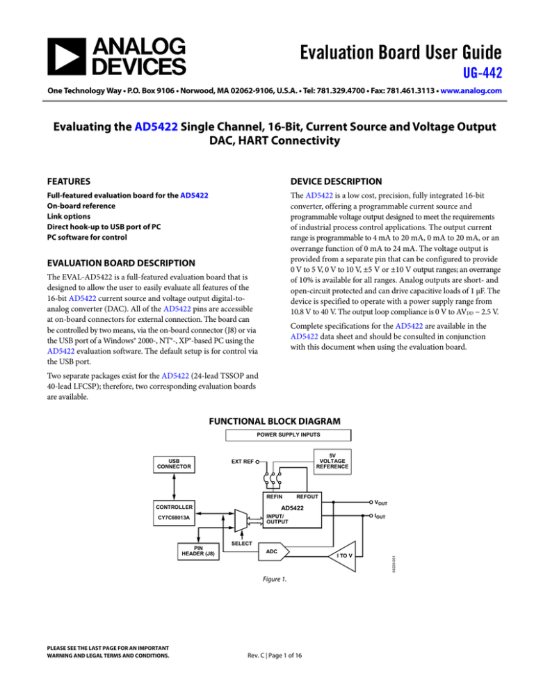
Evaluation Board User Guide UG-442 One Technology Way • P.O. Box 9106 • Norwood, MA 02062-9106, U.S.A. • Tel: 781.329.4700 • Fax: 781.461.3113 • www.analog.com Evaluating the AD5422 Single Channel, 16-Bit, Current Source and Voltage Output DAC, HART Connectivity FEATURES DEVICE DESCRIPTION Full-featured evaluation board for the AD5422 On-board reference Link options Direct hook-up to USB port of PC PC software for control The AD5422 is a low cost, precision, fully integrated 16-bit converter, offering a programmable current source and programmable voltage output designed to meet the requirements of industrial process control applications. The output current range is programmable to 4 mA to 20 mA, 0 mA to 20 mA, or an overrange function of 0 mA to 24 mA. The voltage output is provided from a separate pin that can be configured to provide 0 V to 5 V, 0 V to 10 V, ±5 V or ±10 V output ranges; an overrange of 10% is available for all ranges. Analog outputs are short- and open-circuit protected and can drive capacitive loads of 1 μF. The device is specified to operate with a power supply range from 10.8 V to 40 V. The output loop compliance is 0 V to AVDD − 2.5 V. EVALUATION BOARD DESCRIPTION The EVAL-AD5422 is a full-featured evaluation board that is designed to allow the user to easily evaluate all features of the 16-bit AD5422 current source and voltage output digital-toanalog converter (DAC). All of the AD5422 pins are accessible at on-board connectors for external connection. The board can be controlled by two means, via the on-board connector (J8) or via the USB port of a Windows® 2000-, NT®-, XP®-based PC using the AD5422 evaluation software. The default setup is for control via the USB port. Complete specifications for the AD5422 are available in the AD5422 data sheet and should be consulted in conjunction with this document when using the evaluation board. Two separate packages exist for the AD5422 (24-lead TSSOP and 40-lead LFCSP); therefore, two corresponding evaluation boards are available. FUNCTIONAL BLOCK DIAGRAM POWER SUPPLY INPUTS 5V VOLTAGE REFERENCE EXT REF REFIN CONTROLLER IOUT SELECT ADC Figure 1. PLEASE SEE THE LAST PAGE FOR AN IMPORTANT WARNING AND LEGAL TERMS AND CONDITIONS. VOUT INPUT/ OUTPUT CY7C68013A PIN HEADER (J8) REFOUT AD5422 Rev. C | Page 1 of 16 I TO V 08230-001 USB CONNECTOR UG-442 Evaluation Board User Guide TABLE OF CONTENTS Features .............................................................................................. 1 Link Options ..................................................................................3 Evaluation Board Description......................................................... 1 Evaluation Board Software ...............................................................6 Device Description ........................................................................... 1 Software Installation .....................................................................6 Functional Block Diagram .............................................................. 1 Software Operation .......................................................................6 Revision History ............................................................................... 2 Evaluation Board Schematics and Artwork ...................................8 Evaluation Board Hardware ............................................................ 3 Ordering Information .................................................................... 14 Power Supplies .............................................................................. 3 Bill of Materials ........................................................................... 14 REVISION HISTORY 10/13—Rev. B to Rev. C Change to Figure 6 ........................................................................... 9 Change to Figure 8 ......................................................................... 11 Changes to C3, Supplier/Number Column, Table 5 .................. 14 3/13—Rev. A to Rev. B Change to Control Register Section and Added Figure 4; Renumbered Sequentially ................................................................ 7 7/12—Rev. 0 to Rev. A Document Title Changed from EVAL-AD5422 to UG-442................................................................................. Universal Changes to Evaluation Board Description Section ...................... 1 Changes to Figure 3 .......................................................................... 6 Changes to Figure 4 .......................................................................... 8 Changes to Figure 5 .......................................................................... 9 Inserted Figure 6; Renumbered Sequentially .............................. 10 Inserted Figure 7 ............................................................................. 11 Changes to Figure 8 to Figure 10 .................................................. 12 Inserted Figure 11 to Figure 13 ..................................................... 13 4/09—Revision 0: Initial Version Rev. C | Page 2 of 16 Evaluation Board User Guide UG-442 EVALUATION BOARD HARDWARE POWER SUPPLIES Default Link Option Setup The following external supplies must be provided: • • • • • 5 V between the 5 V and 0 V inputs for the digital supply of the AD5422 and digital circuitry. Alternatively, place LK6 in Position A to power the digital circuitry from the USB port (default). 10.8 V to 40 V between the AVDD and GND inputs for the analog supply of the AD5422. 0 V to −26.4 V between the AVSS and GND inputs for the negative analog supply of the AD5422. (This is only required if a bipolar output voltage range is programmed; otherwise, the negative supply of the AD5422 can be connected to GND by placing LK4 in Position A.) 10.8 V to 16.5 V between the V+ and GND inputs for the analog supply of the AD7321 (on-board analog-to-digital converter [ADC]) and ADR435 (on-board voltage reference). If the analog supply connected to the AVDD input is less than 16.5 V, the AD7321 and ADR435 can be powered from this by placing LK9 in Position A, and the V+ input can be left unconnected. 0 V to −16.5 V between the V− and GND inputs for the negative analog supply of the AD7321 (on-board ADC). If the negative analog supply connected to the AVSS input is less than (magnitude) −16.5 V, the AD7321 can be powered from this by placing LK16 in Position A, and the V− input can be left unconnected. The analog and digital planes are connected at one location, close to the AD5422. It is recommended not to connect GND and DGND elsewhere in the system to avoid ground loop problems. Each supply is decoupled to the relevant ground plane with 10 µF and 0.1 µF capacitors. Each device supply pin is again decoupled with a 10 µF and 0.1 µF capacitor pair to the relevant ground plane. Excessive Power Supply If a power supply in excess of 16.5 V is connected to the AVDD input, LK9 must be in Position B to prevent potential damage to the 5 V voltage reference and to the ADC (see U2 and U6, respectively, in Figure 6). However, if a power supply in excess of −16.5 V is to be connected to the AVSS input, LK16 must be in Position B to prevent potential damage to the ADC. LINK OPTIONS The position of LK7 configures the board for either PC control via the USB port (default setup) or for control by an external source via J8. Set the link options on the evaluation board for the required operating setup before using the board. The functions of the link options are described in Table 4. The default setup is for control by the PC via the USB port. The default link options are listed in Table 1. Table 1. Link and Switch Options for PC Control Link No. LK1 LK2 LK3 LK4 LK5 LK6 LK7 LK8 LK9 LK10 LK11 LK12 LK13 LK14 LK15 LK16 LK17 LK18 Option A A Inserted B B A A A A Inserted Inserted Inserted Inserted Inserted C A Inserted Inserted Connector J8 Pin Descriptions Table 2. Connector J8 Pin Configuration1 2 1 1 4 3 6 5 8 7 LK7 must be in Position B to enable the use of J8. Table 3. Connector J8 Pin Descriptions Connector J8 Pin No. 1 2 3 4 5 6 7 8 9 10 Rev. C | Page 3 of 16 Function SDO CLEAR SELECT DGND CLEAR DGND FAULT SDIN DGND SCLK LATCH 10 9 UG-442 Evaluation Board User Guide Table 4. Link Options Link No. LK1 LK2 LK3 LK4 LK5 LK6 LK7 LK8 LK9 LK10 LK11 LK12 LK13 LK14 Description This link selects the state of the CLEAR SELECT pin (when the evaluation board is configured for external control). Position A ties the CLEAR SELECT pin to 0 V. Position B ties the CLEAR SELECT pin to DVCC. This link selects the state of the CLEAR pin (when the evaluation board is configured for external control). Position A ties the CLEAR pin to 0 V. Position B ties the CLEAR pin to DVCC. This link selects the state of the DVCC SELECT pin. When inserted, the DVCC SELECT pin is tied to 0 V, disabling the internal supply; an external supply must be connected to the DVCC pin via LK17. When removed, the DVCC SELECT pin is unconnected, enabling the internal supply. Removing LK3 eliminates the need for an external digital supply; therefore, LK17 can also be removed. This link selects the negative supply voltage for AVSS. Position A selects 0 V as the negative supply voltage (unipolar voltage output operation). Position B selects the AVSS connection of J2 as the negative supply voltage (bipolar voltage output operation). This link selects how the IOUT current loop return is connected to ground on the evaluation board. Position A connects the IOUT current loop return directly to ground. Position B connects the IOUT current loop return input to GND through a 51 Ω resistor. The high side of the resistor is connected to the VIN1 input of the on-board ADC (AD7321), allowing readback to the PC of the output current. This link selects the 5 V power supply source for the digital circuitry. Position A selects the USB port as the 5 V digital circuitry power supply source. Position B selects J7 as the 5 V digital circuitry power supply source. This link selects whether the AD5422 evaluation board is controlled by the PC via the USB port or by an external source via J8. Position A selects the evaluation board to be controlled by the PC via the USB port. Position B selects the evaluation board to be controlled by an external source via J8. This link selects the digital supply voltage value for the AD5422 and the on-board ADC (U6). Position A selects 5 V as the supply value. Position B selects 3.3 V as the supply value. This link selects the positive power supply source for U2 and U6. Position A selects the AVDD input as the positive power supply source (use only if the power supply applied to AVDD is less than 16.5 V). Position B selects the V+ input as the positive power supply source (use if the power supply applied to AVDD input is greater than 16.5 V). A power supply voltage of 10.8 V to 16.5 V can be applied to V+. This link is used to enable/disable the external boost transistor. When this link is inserted, the external boost transistor is disabled. When this link is removed, the external boost transistor is enabled. This link connects the −VSENSE input to ground. When this link is inserted, the −VSENSE input is connected directly to ground. When this link is removed, the −VSENSE input is left floating and should be connected to the low side of the load resistance external to the evaluation board. This link connects the +VSENSE input to VOUT. When this link is inserted, the +VSENSE input is connected directly to the VOUT pin. When this link is removed, the +VSENSE input is connected to VOUT through a 47 kΩ resistance (to prevent the integrated voltage amplifier loop from opening). This link connects the IOUT connector directly to the GND connector. When this link is inserted, the IOUT connector is connected directly to the GND connector. When this link is removed, the IOUT connector is disconnected from the GND connector (an external load must be connected). This link connects the VOUT output of the AD5422 to the VIN0 input of the on-board ADC (AD7321). When this link is inserted, the voltage at the VOUT pin can be read back to the PC. When this link is removed, the voltage at the VOUT pin is disconnected from the on-board ADC input. Rev. C | Page 4 of 16 Evaluation Board User Guide Link No. LK15 LK16 LK17 LK18 UG-442 Description This link selects the voltage reference source. Position A selects the internal voltage reference of the AD5422 as the voltage reference source. Position B selects an external source that can be applied at Connector J3. Position C selects the on-board ADR435 as the voltage reference source. This link selects the negative power supply source for U6. Position A selects the AVSS input as the negative power supply source (use only if the power supply applied to AVSS input is less (in magnitude) than −16.5 V). Position B selects the V− input as the negative power supply source (use only if the power supply applied to AVSS input is greater (in magnitude) than −16.5 V). This link connects the DVCC pin of the AD5422 to the on-board digital power supply. When this link is inserted, the DVCC pin of the AD5422 is connected to the on-board digital power supply (LK3 must be inserted to disable the AD5422 internal digital power supply). When this link is removed, the DVCC pin of the AD5422 is disconnected from the on-board digital power supply (LK3 should be removed to enable the AD5420 internal digital power supply). This link connects the AVDD pin of the AD5422 to the power supply applied at the AVDD input connector, J2 (LK18 must be inserted for operation of the AD5422). Rev. C | Page 5 of 16 UG-442 Evaluation Board User Guide EVALUATION BOARD SOFTWARE SOFTWARE OPERATION The AD5422 evaluation kit includes self-installing software on a CD. The software is compatible with Windows 2000/NT/XP. If the setup file does not run automatically, run the setup.exe file from the CD. To launch the software, complete the following steps: 1. From the Start menu, select Analog Devices – AD5422/ AD5422 Evaluation Software. The main window of the software then displays (see Figure 3). To install the evaluation software, do the following: 2. If the evaluation board is not connected to the USB port when the software is launched, a connectivity error is displayed (see Figure 2). Simply connect the evaluation board to the USB port of the PC and click Retry. 2. 3. 4. Install the evaluation software before connecting the evaluation board to the USB port of the PC to ensure that the evaluation board is correctly recognized when connected to the PC. After installation from the CD is complete, power up the AD5422 evaluation board as described in the Power Supplies section. Connect the board to the USB port of the PC using the supplied cable. When the evaluation board is detected, proceed through any dialog boxes that appear. This finishes the installation. Figure 2. Connectivity Error Alert 08230-003 1. 08230-002 SOFTWARE INSTALLATION Figure 3. Main Window Rev. C | Page 6 of 16 Evaluation Board User Guide UG-442 The main window is divided into eight sections: Input Register, Status Register, Control Register, Reset Register, Clear/Clear Select Pins, Read/Write Registers, Measure Output Voltage/ Current, and Program Voltage/Current. Reset Register Input Register Clear Pin The Input Register section displays the contents of the input register. The 24-bit display is updated each time a read or a write operation is requested via the main window controls. It allows users to associate the value written to the AD5422 with the various programmable functions. In the Clear/Clear Select Pins section, you can change the state of the CLEAR pin by clicking the CLEAR button. Likewise, you can change the state of the CLEAR SELECT pin by clicking the CLEAR SELECT button. Status Register The Status Register section displays the states of the three bits of the read-only status register. To read the register, click the Read Status Register button. Control Register The Control Register section facilitates programming of the control register on an individual bit basis. To change the value for a bit, click the relevant button. Each button also displays the current state of the bit. You can also enter code in the SR CLOCK and SR STEP text boxes and select an output range from the OUTPUT RANGE drop-down box. When using an external current setting resistor, it is recommended to only set REXT when also setting the OUTEN bit. Alternately, REXT can be set before the OUTEN bit is set, but the range must be changed on the write in which the output is enabled. The Read/Write Registers section should be used for these commands (see Figure 4). The sole function of the Reset Register section is to allow the AD5422 to be reset to its power-on state. To change the value of the reset bit, click the RESET button. Read/Write Registers In the Read/Write Registers section, you can read from and write to all registers in the AD5422. To select a register and request a read or write, click the Select Control Function drop-down box. Then, to write data to the register, select the desired data from the Data Write drop-down box and then click OK. Register data is updated and displayed for you to read in the Data Read text box each time you click OK. Measure Output Voltage/Current To display the programmed output current in the Measure Output Current section, click the Measure output Current button. The output current is measured using the on-board ADC and is displayed in milliamperes in the VOUT or IOUT box. The output current is measured with an accuracy of approximately 1% and is therefore not intended as precise, but rather is an approximate feedback of the programmed value. Program Current To program a voltage or current output value, enter the value in either volts or milliamperes (mA) in the Enter Value text box of the Program Voltage/Current section, and press Enter. The output must first be enabled, and the output range must be selected via the Control Register section. POWER-ON SOFTWARE RESET CONTROL REGISTER WRITE (ONE WRITE COMMAND) • SELECT RSET EXTERNAL/INTERNAL • SET THE REQUIRED RANGE • CONFIGURE THE SLEW RATE CONTROL (IF REQUIRED) • CONFIGURE DAISY CHAIN MODE (IF REQUIRED) • ENABLE THE OUTPUT CONTROL REGISTER WRITE • DISABLE OUTPUT DATA REGISTER WRITE RSET CONFIGURATION CHANGE RANGE CHANGE Figure 4. Programming Sequence to Write/Enable the Output Correctly Rev. C | Page 7 of 16 08230-300 • WRITE REQUIRED CODE TO DATA REGISTER DGND DVCC PGND SHIELD J7-2 C55 PA2 PA3 PA5 PA6 PA7 FD8 FD7 LK1 LK2 PGND DVCC DVCC DGND DVCC 10µF + C56 USB_POWER J1 USB-MINI-B 1 VBUS 2 D– 3 D+ 4 IO 5 GND 0.1µF B A VDD S1A S2A S3A S4A DGND 2 5 11 14 16 U8 D1 R23 1kΩ 5V PGND RED 1 15 4 7 9 12 ADG774 DGND 8 D1 D2 D3 D4 IN EN GND + U7 2 5 11 14 16 0.1µF 10µF DVCC 20% C19 VDD PGND ADP3303-3.3 8 OUT1 7 IN1 OUT2 5 IN2 SD ERROR NR GND C18 U3 4 PGND 0V B A LK6 3 S1B 6 S2B 10 S3B 13 S4B PGND DGND EXT_5V S1A S2A S3A S4A C28 0.1µF R16 100kΩ 15 ADG774 DGND 8 4 7 9 12 R17 100kΩ PGND R20 10kΩ C57 3.3V PGND SDIN SCLK LATCH FAULT SDO CLEAR_SELECT CLEAR PGND R22 10kΩ 13 14 1 2 33 34 35 36 37 38 39 40 9 8 54 42 44 C31 2.2µF RDY0/*SLRD RDY1/*SLWR PA0/INT0 PA1/INT1 PA2/*SLOE PA3/*WU2 PA4/FIFOADR0 PA5/FIFOADR1 PA6/*PKTEND PA7/*FLD/SLCS PGND IFCLK RSVD LK8 3.3V U4 D– D+ CY7C68013-CS P CLKOUT RESET *WAKEUP 3.3V R18 0Ω PGND PGND 0.1µF C30 PGND 0.1µF R21 10kΩ PA5 PA6 PA7 PA2 PA3 CS_ADC PGND C29 0.1µF 3.3V 0.1µF PGND R19 10kΩ D1 D2 D3 D4 IN EN GND 1 C20 PGND 3.3V 1 2 6 3 3 S1B 6 S2B 10 S3B 13 S4B B A FAULT SDO CLEAR_SELECT DGND CLEAR DGND SDIN DGND SCLK LATCH J8-6 J8-1 J8-2 J8-3 J8-4 J8-5 J8-7 J8-8 J8-9 J8-10 3 AVCC +5V B AGND 6 A B 7 11 17 27 32 43 55 J7-1 DGND PGND XTALIN XTALOUT SDA SCL CTL0/*FLAGA CTL1/*FLAGB CTL2/*FLAGC PB0/FD0 PB1/FD1 PB2/FD2 PB3/FD3 PB4/FD4 PB5/FD5 PB6/FD6 PB7/FD7 PD0/FD8 PD1/FD9 PD2/FD10 PD3/FD11 PD4/FD12 PD5/FD13 PD6/FD14 PD7/FD15 C32 22pF 5 4 16 15 29 30 31 18 19 20 21 22 23 24 25 45 46 47 48 49 50 51 52 DVCC 24 MHz PGND Y2 SDIN_ADC SCLK_ADC DOUT_ADC FD7 FD8 C22 C33 22pF R24 2.2kΩ C23 R25 2.2kΩ 0.1µF 3.3V PGND 0.1µF PGND 3.3V 0.1µF C21 3.3V C24 3.3V C25 C26 C34 0.1µF C27 U5 1 2 3 4 0.1µF 24LC64 8 A0 7 VCC WP A1 6 A2 5 SCL SDA VSS 0.1µF 0.1µF PGND 0.1µF PGND 3.3V PGND 08230-004 VCC VCC VCC VCC VCC VCC VCC GND GND GND GND GND GND GND 10 12 26 28 41 53 56 Rev. C | Page 8 of 16 A Figure 5. AD5422 TSSOP Evaluation Board Schematic of the Controller Circuitry LK7 UG-442 Evaluation Board User Guide EVALUATION BOARD SCHEMATICS AND ARTWORK V+ B 0Ω 0Ω 0Ω 0Ω 0Ω 0Ω R8 R9 R6 R5 R10 R4 1 2 14 12 11 10µF DVCC 0.1µF CS DIN SCLK DOUT DGND VDRIVE U6 C35 C36 DGND 20% LK16 B C45 DGND 10kΩ R14 10kΩ R3 DVCC C43 A C46 C44 VIN1 AD7321 VIN0 0.1µF 10µF 10µF 0.1µF 8 7 5 2 B 15 C 24 VIN0 4 12 U1 6 11 C49 C48 R13 39kΩ + AD820 – 4 V– 7 V+ C10 0.1µF 1 2 3 U9 R1 15kΩ R27 20% 0.1µF 10µF C8 + C9 LK18 SOCKETED 4nF C1 AVSS 13 19 20 23 21 22 18 17 R12 5.6kΩ 0.1µF 10µF 10µF C11 AVSS RSET IOUT BOOST –VSENSE VOUT +VSENSE CCOMP2 CCOMP1 AD5422_TSSOP GND GND GND LATCH SCLK SDIN SDO CLEAR_SELECT CLEAR FAULT DVCC_SELECT 10µF C47 20% 0.1µF AVSS V– 14 J3 REFIN 6 0.1µF DVCC REFOUT REFIN AVDD + C50 7 8 9 10 5 6 3 16 DGND 2 4 VOUT U2 ADR435 TRIM GND +VIN + C16 C15 20% 1µF 0.1µF LK3 LK17 + C42 C41 20% 10µF 0.1µF SOCKETED C3 22nF LK10 V– LK14 1kΩ R2 AVDD V+ Q1 V+ LK11 R11 51Ω V– 0.1µF C40 0.1µF C39 LK12 VIN0 + C38 20% 10µF + C37 20% 10µF NOTES 1. PIN 18 IS LISTED AS NC IN THE AD5422 DATA SHEET AND CCOMP2 IN THIS SCHEMATIC. CONNECTING THE COMPENSATION CAPACITOR BETWEEN PIN 17 AND PIN 18 OR PIN 17 AND PIN 21 HAS THE SAME EFFECT. NEW DESIGNS MUST FOLLOW THE AD5422 DATA SHEET RECOMMENDATIONS OF INSERTING THE COMPENSATION CAPACITOR BETWEEN CCOMP AND VOUT. CS_ADC SDIN_ADC SCLK_ADC DOUT_ADC LATCH SCLK SDIN SDO CLEAR_SELECT CLEAR FAULT 0Ω R7 DVCC TP1 TP2 TP3 TP4 TP5 TP6 TP7 D2 RED 1kΩ R26 C12 + LK15 A THE FOLLOWING COMPONENTS ARE NOT TO BE POPULATED : C12, C14, C17, C52, C53, R27 TP8 TP9 TP10 TP11 C14 10 VCC DGND DGND 13 3 20% R15 4.7kΩ J6-2 J6-1 LK5 LK13 AVSS AVDD J13-1 J12-1 J11-1 J10-1 J9-1 B C6 J5-2 J5-1 J4-3 J4-2 X1 AVSS AGND AVDD J2-1 J2-2 J2-3 CLAMP-SOIC-TSSOP GND IOUT –VSENSE VOUT J4-1 10µF 0.1µF C7 C4 + C5 20% 10µF 0.1µF +VSENSE A A LK9 680nF C51 5 REFIN/OUT C17 AGND 4 9 VDD VSS 6 + 20% Figure 6. AD5422 TSSOP Evaluation Board Schematic of the AD5422 Circuitry + B C13 20% + Rev. C | Page 9 of 16 A LK4 AVDD 08230-005 C6,C7,C10,C11 MUST BE RATED OVER 30V C4,C5,C8,C9 MUST BE RATED OVER 60V Evaluation Board User Guide UG-442 DVCC 0.1µF C55 LK1 PA2 PA3 PA5 PA6 PA7 FD8 FD7 DGND PGND IO 5 4 LK2 DVCC DVCC DGND DVCC GND 10µF + C56 U8 VDD 2 5 S1A S2A 11 14 S3A S4A 16 PGND USB_POWER J1 USB-MINI-B 1 VBUS 2 DSHIELD SHIELD 3 D+ J7-2 0V B A LK6 DGND D1 R23 1kΩ 5V D1 D2 D3 D4 4 7 9 12 DGND C28 0.1µF R16 100kΩ C20 R19 10kΩ PGND 3.3V 1 2 6 3 DGND C30 PGND PGND PGND SDIN SCLK LATCH LK8 3.3V PGND 1 2 RDY0/*SLRD RDY1/*SLWR 13 14 IFCLK RSVD RESET *WAKEUP PGND PGND XTALIN XTALOUT DGND 29 30 31 18 19 20 21 22 23 24 25 45 46 47 48 49 50 51 52 DVCC 5 4 16 SDA 15 SCL PB0/FD0 PB1/FD1 PB2/FD2 PB3/FD3 PB4/FD4 PB5/FD5 PB6/FD6 54 CLKOUT PB7/FD7 PD0/FD8 PD1/FD9 9 U4 PD2/FD10 D8 D+ CY7C68013-CSP PD3/FD11 PD4/FD12 PD5/FD13 33 PD6/FD14 34 PA0/INT0 PD7/FD15 35 PA1/INT1 PA2/*SLOE 36 PA3/*WU2 37 PA4/FIFOADR0 CTL0/*FLAGA 38 CTL1/*FLAGB 39 PA5/FIFOADR1 CTL2/*FLAGC 40 PA6/*PKTEND PA7/*FLD/SLCS 42 44 FAULT SDO CLEAR_SELECT CLEAR R22 10kΩ PGND PGND R21 10kΩ PA5 PA6 PA7 PA2 PA3 CS_ADC PGND 3.3V 2.2µF C31 R18 0Ω PGND 3.3V 0.1µF C29 0.1µF 0.1µF R17 100kΩ 3.3V 0.1µF C57 R20 10kΩ 4 D1 7 D2 9 D3 12 D4 IN EN GND 1 15 8 ADG774 VDD 2 5 S1A 11 S2A 14 S3A S4A 16 U7 ADP3303-3.3 8 OUT1 7 IN1 OUT2 5 IN2 SD ERROR GND NR + C19 C18 U3 4 20% 10µF 0.1µF PGND DVCC PGND RED IN EN GND ADG774 115 8 3 S1B 6 S2B 10 S3B 13 S4B EXT_5V PGND B A FAULT SDO CLEAR_SELECT DGND CLEAR DGND SDIN DGND SCLK LATCH J8-6 J8-1 J8-2 J8-3 J8-4 J8-5 J8-7 J8-8 J8-9 J8-10 PGND DGND +5V B A AGND 6 J7-1 B 3 S1B 6 S2B 10 S3B 13 S4B 3 AVCC A B 7 11 17 27 32 43 55 VCC VCC VCC VCC VCC VCC VCC GND GND GND GND GND GND GND 10 12 26 28 41 53 56 Rev. C | Page 10 of 16 A Figure 7. AD5422 LFCSP Evaluation Board Schematic of the Controller Circuitry LK7 PGND C32 22pF 24 MHz Y2 SDIN_ADC SCLK_ADC DOUT_ADC FD7 FD8 PGND C33 22pF R24 2.2kΩ 3.3V C22 C23 C24 C25 C26 C27 R25 2.2kΩ 3.3V PGND C34 U5 24LC64 8 A0 7 VCC WP A1 6 A2 5 SCL VSS SDA 0.1µF PGND 3.3V 1 2 3 4 PGND 0.1µF 0.1µF 0.1µF 0.1µF 0.1µF 0.1µF 0.1µF C21 3.3V PGND 3.3V UG-442 Evaluation Board User Guide 08230-006 VDRIVE 0.1µF DGND 1 2 CS 14 DIN 12 SCLK DOUT 11 U6 C35 C36 10µF DVCC LK16 B C45 C43 A C46 C44 VIN1 AD7321 VIN0 8 10µF 0.1µF 7 0.1µF 10µF V– AVSS 17 J3 18 B 36 IOUT BOOST -VSENSE VOUT +VSENSE CCOMP2 CCOMP1 CAP2 CAP1 VIN0 3 6 15 13 12 C49 37 V+ C48 R13 39kΩ + AD820 – 4 V– 7 C10 0.1µF 14 10µF C11 RSET GNDGNDGNDGND AVSS AVSS LATCH SCLK SDIN SDO CLEAR_SELECT CLEAR FAULT U1 AD5422 DVCC_SELECT DVCC REFOUT REFIN AVDD 39 6 REFIN 10µF C47 20% + C50 0.1µF 6 7 8 9 0Ω 0Ω 0Ω 0Ω R6 R5 R10 R4 DGND 4 5 23 0Ω 0Ω LK3 DGND R8 R9 10kΩ R14 4 + C16 C15 20% 1µF 0.1µF 2 10kΩ R3 DVCC LK17 VOUT U2 ADR435 TRIM GND +VIN 0Ω DGND 2 + C42 C41 20% 10µF 0.1µF 5 TP1 TP2 TP3 TP4 TP5 TP6 TP7 20% C 2 3 U9 R12 5.6kΩ 0.1µF 10µF AVSS 16 26 27 34 32 33 25 24 29 28 4nF R1 15kΩ SOCKETED C1 C53 C52 C3 22nF V– AVDD LK14 1kΩ R2 LK10 R27 SOCKETED SOCKETED C8 + C9 20% 0.1µF 10µF LK18 V+ NOTES 1. PIN 25 IS LISTED AS NC IN THE AD5422 DATA SHEET AND CCOMP2 IN THIS SCHEMATIC. CONNECTING THE COMPENSATION CAPACITOR BETWEEN PIN 24 AND PIN 25 OR PIN 24 AND PIN 32 HAS THE SAME EFFECT. NEW DESIGNS MUST FOLLOW THE AD5422 DATA SHEET RECOMMENDATIONS OF INSERTING THE COMPENSATION CAPACITOR BETWEEN CCOMP AND VOUT. CS_ADC SDIN_ADC SCLK_ADC DOUT_ADC LATCH SCLK SDIN SDO CLEAR_SELECT CLEAR B R7 TP8 TP9 TP10 TP11 C12 + FAULT RED D2 1kΩ R26 LK9 DVCC C17 LK15 A A C14 VCC 680nF C51 5 REFIN/OUT 10 13 3 DGND DGND 20% 0.1µF C13 20% Q1 LK11 LK12 VIN0 + C38 20% 10µF 0.1µF C40 C39 + C37 20% 10µF 0.1µF V– V+ AVSS R11 51Ω R15 4.7kΩ J6-2 J6-1 AVDD LK5 LK4 V+ VSS 6 AGND 4 9 VDD + 20% Figure 8. AD5422 LFCSP Evaluation Board Schematic of the AD5422 Circuitry + + B C6 J13-1 J12-1 J11-1 J10-1 J9-1 AVSS GND IOUT -VSENSE VOUT +VSENSE 10µF0.1µF C7 AGND AVDD C4 + C5 20% 10µF 0.1µF LK13 A B A Rev. C | Page 11 of 16 J5-2 J5-1 J4-3 J4-2 J4-1 J2-1 J2-2 J2-3 08230-007 AVDD Evaluation Board User Guide UG-442 Evaluation Board User Guide 08230-008 UG-442 08230-009 Figure 9. AD5422 TSSOP Evaluation Board Component Placement 08230-010 Figure 10. AD5422 TSSOP Evaluation Board Solder Side PCB Figure 11. AD5422 TSSOP Evaluation Board Component Side PCB Rev. C | Page 12 of 16 UG-442 08230-011 Evaluation Board User Guide 08230-012 Figure 12. AD5422 LFCSP Evaluation Board Component Placement 08230-013 Figure 13. AD5422 LFCSP Evaluation Board Solder Side PCB Figure 14. AD5422 LFCSP Evaluation Board Component Side PCB Rev. C | Page 13 of 16 UG-442 Evaluation Board User Guide ORDERING INFORMATION BILL OF MATERIALS Table 5. Qty 1 Reference Designator U1 1 1 1 U2 U3 U4 1 1 2 1 1 2 2 2 2 25 U5 U6 U7, U8 U9 C3 C4, C8 C5, C9 C6, C10 C7, C11 C13, C15, C18, C20, C21, C22, C23, C24, C25, C26, C27, C28, C29, C30, C34, C35, C39, C40, C41, C43, C44, C47, C48, C55, C57 C16 C19, C36, C37, C38, C42, C45, C46, C49, C50, C56 C31 C32, C33 C51 LK1, LK2, LK4, LK5, LK6, LK7, LK8, LK9, LK16 LK3, LK10, LK11, LK12, LK13, LK14, LK17, LK18 LK15 J1 J2, J4 J3 J5, J6, J7 J8 D1, D2 TP1 to TP11 R1 R2, R23, R26 R3, R14, R19, R20, R21, R22 R4 to R10, R18 R11 R12 R13 R15 R16, R17 R24, R25 Y2 Q1 1 10 1 2 1 9 8 1 1 2 1 3 1 2 11 1 3 6 8 1 1 1 1 2 2 1 1 Description 16-bit current source DAC (TSSOP Package) 16-bit current source DAC (LFCSP Package) 5 V voltage reference 3.3 V low dropout voltage regulator USB microcontroller 64 K EEPROM 12-bit ADC Quad 2:1 multiplexer Low noise, precision operational amplifier 22 nF, 16 V X7R ceramic capacitor 0.1 µF, 100 V ceramic capacitor 10 µF, 63 V (FK series) electrolytic capacitor 0.1 µF, 50 V, X7R ceramic capacitor 10 µF, 35 V, Y5V ceramic capacitor 0.1 µF, 16 V X7R ceramic capacitor Supplier/Number Analog Devices/AD5422BREZ Analog Devices/AD5422BCPZ Analog Devices/ADR435ARZ Analog Devices/ADP3303ARZ-3.3 Cypress Semiconductor/ CY7C68013-56LFXC Digi-Key/24LC64-I/SN-ND Analog Devices/AD7321BRUZ Analog Devices/ADG774BRQZ Analog Devices/OP27GSZ FEC 165-8869 FEC 1288275 FEC 9696008 FEC 1288255 Digi-Key/587-1352-1-ND FEC 1216538 1 µF, 10 V SMD tantalum capacitor 10 µF SMD tantalum capacitor FEC 197099 2.2 µF, 10 V, Y5V ceramic capacitor 22 pF, 50 V NPO ceramic capacitor 680 nF, 16 V, Y5V ceramic capacitor 3-pin (0.1" pitch) header and jumper socket 2-pin (0.1" pitch) header and jumper socket FEC 9402098 FEC 722005 Digi-Key/490-1581-1-ND FEC 1022249 and FEC 150-411 FEC 1022247 FEC 150-411 6-pin (3 × 2) 0.1" header and jumper socket USB mini-B connector 3-pin terminal block (5 mm pitch) 50 Ω SMB jack 2-pin terminal block (5 mm pitch) 2-row, 36 + 36 header Red SMD LED Black test point 15 kΩ SMD precision resistor 1 kΩ SMD resistor 10 kΩ SMD resistor 0 Ω SMD resistor 51 Ω SMD resistor 5.6 kΩ SMD resistor 39 kΩ SMD resistor 4.7 kΩ SMD resistor 100 kΩ SMD resistor 2.2 kΩ SMD resistor 24 MHz plastic SMD crystal NPN transistor, PBSS8110Z FEC 1022231 and FEC 150411 FEC 9786490 FEC 151790 FEC 1111349 FEC 151789 FEC 1022244 (36 + 36 pin strip) FEC 5790840 FEC 8731128 FEC 1140932 FEC 9330380 FEC 9330399 FEC 9331662 FEC 9331336 FEC 9331352 FEC 9331158 FEC 9331247 FEC 9330402 FEC 9330810 FEC 9509658 FEC 8736677 Rev. C | Page 14 of 16 Evaluation Board User Guide UG-442 NOTES Rev. C | Page 15 of 16 UG-442 Evaluation Board User Guide NOTES ESD Caution ESD (electrostatic discharge) sensitive device. Charged devices and circuit boards can discharge without detection. Although this product features patented or proprietary protection circuitry, damage may occur on devices subjected to high energy ESD. Therefore, proper ESD precautions should be taken to avoid performance degradation or loss of functionality. Legal Terms and Conditions By using the evaluation board discussed herein (together with any tools, components documentation or support materials, the “Evaluation Board”), you are agreeing to be bound by the terms and conditions set forth below (“Agreement”) unless you have purchased the Evaluation Board, in which case the Analog Devices Standard Terms and Conditions of Sale shall govern. Do not use the Evaluation Board until you have read and agreed to the Agreement. Your use of the Evaluation Board shall signify your acceptance of the Agreement. This Agreement is made by and between you (“Customer”) and Analog Devices, Inc. (“ADI”), with its principal place of business at One Technology Way, Norwood, MA 02062, USA. Subject to the terms and conditions of the Agreement, ADI hereby grants to Customer a free, limited, personal, temporary, non-exclusive, non-sublicensable, non-transferable license to use the Evaluation Board FOR EVALUATION PURPOSES ONLY. Customer understands and agrees that the Evaluation Board is provided for the sole and exclusive purpose referenced above, and agrees not to use the Evaluation Board for any other purpose. Furthermore, the license granted is expressly made subject to the following additional limitations: Customer shall not (i) rent, lease, display, sell, transfer, assign, sublicense, or distribute the Evaluation Board; and (ii) permit any Third Party to access the Evaluation Board. As used herein, the term “Third Party” includes any entity other than ADI, Customer, their employees, affiliates and in-house consultants. The Evaluation Board is NOT sold to Customer; all rights not expressly granted herein, including ownership of the Evaluation Board, are reserved by ADI. CONFIDENTIALITY. This Agreement and the Evaluation Board shall all be considered the confidential and proprietary information of ADI. Customer may not disclose or transfer any portion of the Evaluation Board to any other party for any reason. Upon discontinuation of use of the Evaluation Board or termination of this Agreement, Customer agrees to promptly return the Evaluation Board to ADI. ADDITIONAL RESTRICTIONS. Customer may not disassemble, decompile or reverse engineer chips on the Evaluation Board. Customer shall inform ADI of any occurred damages or any modifications or alterations it makes to the Evaluation Board, including but not limited to soldering or any other activity that affects the material content of the Evaluation Board. Modifications to the Evaluation Board must comply with applicable law, including but not limited to the RoHS Directive. TERMINATION. ADI may terminate this Agreement at any time upon giving written notice to Customer. Customer agrees to return to ADI the Evaluation Board at that time. LIMITATION OF LIABILITY. THE EVALUATION BOARD PROVIDED HEREUNDER IS PROVIDED “AS IS” AND ADI MAKES NO WARRANTIES OR REPRESENTATIONS OF ANY KIND WITH RESPECT TO IT. ADI SPECIFICALLY DISCLAIMS ANY REPRESENTATIONS, ENDORSEMENTS, GUARANTEES, OR WARRANTIES, EXPRESS OR IMPLIED, RELATED TO THE EVALUATION BOARD INCLUDING, BUT NOT LIMITED TO, THE IMPLIED WARRANTY OF MERCHANTABILITY, TITLE, FITNESS FOR A PARTICULAR PURPOSE OR NONINFRINGEMENT OF INTELLECTUAL PROPERTY RIGHTS. IN NO EVENT WILL ADI AND ITS LICENSORS BE LIABLE FOR ANY INCIDENTAL, SPECIAL, INDIRECT, OR CONSEQUENTIAL DAMAGES RESULTING FROM CUSTOMER’S POSSESSION OR USE OF THE EVALUATION BOARD, INCLUDING BUT NOT LIMITED TO LOST PROFITS, DELAY COSTS, LABOR COSTS OR LOSS OF GOODWILL. ADI’S TOTAL LIABILITY FROM ANY AND ALL CAUSES SHALL BE LIMITED TO THE AMOUNT OF ONE HUNDRED US DOLLARS ($100.00). EXPORT. Customer agrees that it will not directly or indirectly export the Evaluation Board to another country, and that it will comply with all applicable United States federal laws and regulations relating to exports. GOVERNING LAW. This Agreement shall be governed by and construed in accordance with the substantive laws of the Commonwealth of Massachusetts (excluding conflict of law rules). Any legal action regarding this Agreement will be heard in the state or federal courts having jurisdiction in Suffolk County, Massachusetts, and Customer hereby submits to the personal jurisdiction and venue of such courts. The United Nations Convention on Contracts for the International Sale of Goods shall not apply to this Agreement and is expressly disclaimed. ©2009–2013 Analog Devices, Inc. All rights reserved. Trademarks and registered trademarks are the property of their respective owners. UG08230-0-10/13(C) Rev. C | Page 16 of 16
