Document 11689329
advertisement
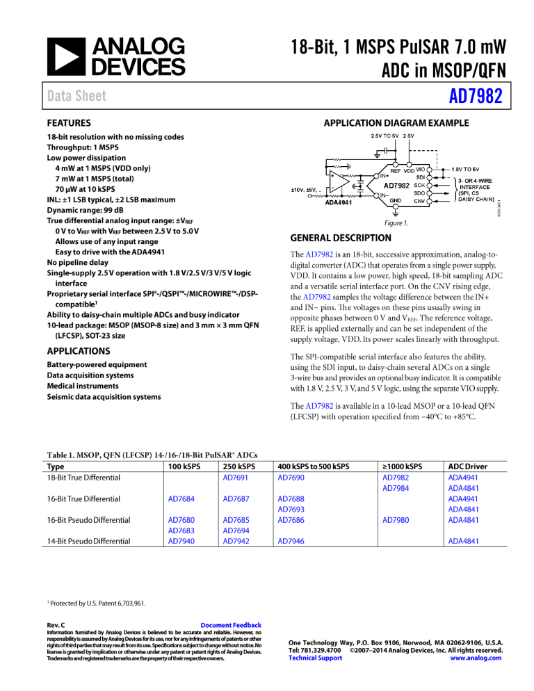
AD7982 Data Sheet TABLE OF CONTENTS Features .............................................................................................. 1 Driver Amplifier Choice ........................................................... 14 Applications ....................................................................................... 1 Single-to-Differential Driver .................................................... 15 Application Diagram Example........................................................ 1 Voltage Reference Input ............................................................ 15 General Description ......................................................................... 1 Power Supply............................................................................... 15 Revision History ............................................................................... 2 Digital Interface .......................................................................... 16 Specifications..................................................................................... 3 CS Mode, 3-Wire Without Busy Indicator ............................. 17 Timing Specifications .................................................................. 5 CS Mode, 3-Wire with Busy Indicator .................................... 18 Absolute Maximum Ratings............................................................ 6 CS Mode, 4-Wire Without Busy Indicator ............................. 19 ESD Caution .................................................................................. 6 CS Mode, 4-Wire with Busy Indicator .................................... 20 Pin Configurations and Function Descriptions ........................... 7 Chain Mode Without Busy Indicator ...................................... 21 Terminology ...................................................................................... 8 Chain Mode with Busy Indicator ............................................. 22 Typical Performance Characteristics ............................................. 9 Application Hints ........................................................................... 23 Theory of Operation ...................................................................... 12 Layout .......................................................................................... 23 Circuit Information .................................................................... 12 Evaluating AD7982 Performance............................................. 23 Converter Operation .................................................................. 12 Outline Dimensions ....................................................................... 24 Typical Connection Diagram ................................................... 13 Ordering Guide .......................................................................... 24 Analog Inputs .............................................................................. 14 REVISION HISTORY 6/14—Rev. B to Rev. C 10/07—Rev. 0 to Rev. A Added Patent Footnote .................................................................... 1 Changes to Table 1 and Layout ........................................................1 Changes to Table 2.............................................................................3 Changes to Layout .............................................................................5 Changes to Layout .............................................................................6 Changes to Figure 5 ...........................................................................7 Changes to Figure 18 and Figure 20............................................. 11 Changes to Figure 23...................................................................... 13 Changers to Figure 26 .................................................................... 15 Changes to Digital Interface Section ........................................... 16 Changes to Figure 38...................................................................... 21 Changes to Figure 40...................................................................... 22 Updated Outline Dimensions ....................................................... 24 Changes to Ordering Guide .......................................................... 24 7/13—Rev. A to Rev. B Added Low Power Dissipation of 4 mW at 1 MSPS (VDD only) to Features Section............................................................................ 1 Changes to Power Dissipation; Table 3 .......................................... 4 Added EPAD Notation to Figure 5 and Table 6 ........................... 7 Updated Outline Dimensions ....................................................... 24 Changes to Ordering Guide .......................................................... 24 3/07—Revision 0: Initial Version Rev. C | Page 2 of 24 Data Sheet AD7982 TIMING SPECIFICATIONS TA = −40°C to +85°C, VDD = 2.37 V to 2.63 V, VIO = 2.3 V to 5.5 V, unless otherwise noted.1 Table 4. Parameter Conversion Time: CNV Rising Edge to Data Available Acquisition Time Time Between Conversions CNV Pulse Width (CS Mode) SCK Period (CS Mode) VIO Above 4.5 V VIO Above 3 V VIO Above 2.7 V VIO Above 2.3 V SCK Period (Chain Mode) VIO Above 4.5 V VIO Above 3 V VIO Above 2.7 V VIO Above 2.3 V SCK Low Time SCK High Time SCK Falling Edge to Data Remains Valid SCK Falling Edge to Data Valid Delay VIO Above 4.5 V VIO Above 3 V VIO Above 2.7 V VIO Above 2.3 V CNV or SDI Low to SDO D15 MSB Valid (CS Mode) VIO Above 3 V VIO Above 2.3 V CNV or SDI High or Last SCK Falling Edge to SDO High Impedance (CS Mode) SDI Valid Setup Time from CNV Rising Edge SDI Valid Hold Time from CNV Rising Edge (CS Mode) SDI Valid Hold Time from CNV Rising Edge (Chain Mode) SCK Valid Setup Time from CNV Rising Edge (Chain Mode) SCK Valid Hold Time from CNV Rising Edge (Chain Mode) SDI Valid Setup Time from SCK Falling Edge (Chain Mode) SDI Valid Hold Time from SCK Falling Edge (Chain Mode) SDI High to SDO High (Chain Mode with Busy Indicator) Min 500 290 1000 10 Typ Max 710 Unit ns ns ns ns 10.5 12 13 15 ns ns ns ns 11.5 13 14 16 4.5 4.5 3 ns ns ns ns ns ns ns tSCK tSCKL tSCKH tHSDO tDSDO 9.5 11 12 14 ns ns ns ns 10 15 20 ns ns ns ns ns ns ns ns ns ns ns tEN tDIS tSSDICNV tHSDICNV tHSDICNV tSSCKCNV tHSCKCNV tSSDISCK tHSDISCK tDSDOSDI 5 2 0 5 5 2 3 15 See Figure 2 and Figure 3 for load conditions. IOL Y% VIO1 X% VIO1 tDELAY 1.4V TO SDO CL 20pF 500µA IOH tDELAY VIH2 VIL2 VIH2 VIL2 1FOR VIO ≤ 3.0V, X = 90, AND Y = 10; FOR VIO > 3.0V, X = 70, AND Y = 30. 2MINIMUM V AND MAXIMUM V USED. SEE DIGITAL INPUTS IH IL SPECIFICATIONS IN TABLE 3. Figure 2. Load Circuit for Digital Interface Timing Figure 3. Voltage Levels for Timing Rev. C | Page 5 of 24 06513-003 500µA 06513-002 1 Symbol tCONV tACQ tCYC tCNVH tSCK REF 1 9 SDI 8 SCK IN– 4 7 SDO GND 5 6 CNV IN+ 3 10 VIO VDD 2 AD7982 9 SDI IN+ 3 TOP VIEW (Not to Scale) 8 SCK 7 SDO 6 CNV IN– 4 GND 5 06513-004 REF 1 AD7982 TOP VIEW NOTES 1. THE EXPOSED PAD SHOULD BE CONNECTED TO GND. THIS CONNECTION IS NOT REQUIRED TO MEET THE ELECTRICAL PERFORMANCES. 06513-005 10 VIO VDD 2 2.0 POSITIVE INL: +0.79 LSB NEGATIVE INL: –0.68 LSB 1.5 1.5 1.0 1.0 0.5 0.5 DNL (LSB) –0.5 0 –0.5 –1.0 –1.5 –1.5 0 65536 131072 CODE 196608 262144 –2.0 0 131072 CODE 40000 35000 40000 COUNTS 32476 29064 30000 20000 30000 25000 20013 20000 16682 15000 10000 10000 9064 7795 0 3FFF0 0 29 3FFF2 745 881 3FFF4 3FFF6 3FFF8 43 3FFFA 0 0 3FFFC CODE IN HEX 06513-007 5000 0 0 7 145 0 1 2 3 4 5 6 7 8 9 222 7 0 0 A B C D 100 SNR (dB REFERRED TO FULL SCALE) fS = 1MSPS fIN = 2kHz –20 SNR = 97.3dB THD = –121.8dB SFDR = 120.2dB SINAD = 97.3dB –40 –60 –80 –100 –120 –140 –160 –180 100 200 300 FREQUENCY (kHz) 400 500 06513-008 AMPLITUDE (dB OF FULL SCALE) 3158 2793 0 CODE IN HEX 0 0 262144 44806 43239 45000 50975 50000 0 196608 50000 60000 COUNTS 65536 06513-010 –2.0 06513-006 –1.0 06513-009 0 POSITIVE INL: +0.46 LSB NEGATIVE INL: –0.49 LSB 99 98 97 96 95 94 93 92 91 90 –10 –9 –8 –7 –6 –5 –4 –3 INPUT LEVEL (dB) –2 –1 0 06513-032 INL (LSB) 2.0 98 –117 96 –119 THD (dB) –115 94 –15 5 25 45 65 TEMPERATURE (°C) 85 105 125 –125 –55 06513-042 –35 –35 –15 5 25 45 65 TEMPERATURE (°C) 85 105 125 06513-041 –123 92 90 –55 –121 1000 06513-030 SNR (dB) 100 –80 100 –85 –90 95 THD (dB) 90 –100 –105 –110 85 –115 –120 80 0.1 1 10 FREQUENCY (kHz) 100 1000 06513-031 SINAD (dB) –95 –125 0.1 1 10 FREQUENCY (kHz) 100 Data Sheet AD7982 1.4 1.4 IVDD IVDD 1.2 OPERATING CURRENTS (mA) 1.0 0.8 0.6 IREF 0.4 IVIO 0.2 2.475 2.525 SUPPLY VOLTAGE (V) 2.575 2.625 06513-036 2.425 Figure 18. Operating Currents vs. Supply Voltage 0.6 IREF 0.4 IVIO 7 6 5 4 3 IVDD + IVIO 2 –15 5 25 45 65 TEMPERATURE (°C) 85 105 125 06513-038 1 –35 0 –55 –35 –15 5 25 45 65 TEMPERATURE (°C) 85 105 Figure 20. Operating Currents vs. Temperature 8 POWER-DOWN CURRENTS (µA) 0.8 0.2 0 2.375 0 –55 1.0 Figure 19. Power-Down Currents vs. Temperature Rev. C | Page 11 of 24 125 06513-035 OPERATING CURRENTS (mA) 1.2 IN+ SWITCHES CONTROL MSB REF 131,072C 65,536C LSB 4C 2C C SW+ C BUSY COMP GND 131,072C 65,536C MSB 4C 2C C CONTROL LOGIC C OUTPUT CODE LSB SW– IN– 06513-011 CNV Data Sheet AD7982 Transfer Functions Table 7. Output Codes and Ideal Input Voltages Description FSR – 1 LSB Midscale + 1 LSB Midscale Midscale – 1 LSB –FSR + 1 LSB –FSR 011...111 011...110 011...101 1 2 100...010 Analog Input VREF = 5 V +4.999962 V +38.15 μV 0V −38.15 μV −4.999962 V −5 V Digital Output Code (Hex) 0x1FFFF1 0x00001 0x00000 0x3FFFF 0x20001 0x200002 This is also the code for an overranged analog input (VIN+ − VIN− above VREF − VGND). This is also the code for an underranged analog input (VIN+ − VIN− below VGND). TYPICAL CONNECTION DIAGRAM 100...001 100...000 –FSR –FSR + 1 LSB –FSR + 0.5 LSB +FSR – 1 LSB +FSR – 1.5 LSB ANALOG INPUT Figure 23 shows an example of the recommended connection diagram for the AD7982 when multiple supplies are available. 06513-012 Figure 22. ADC Ideal Transfer Function V+ REF1 2.5V 10µF2 100nF V+ 1.8V TO 5V 100nF 20Ω 0 TO VREF REF 2.7nF VDD V– AD7982 4 V+ 20Ω ADA48412, 3 SCK SDO IN– VREF TO 0 VIO SDI IN+ GND 3-WIRE INTERFACE CNV 2.7nF V– 4 NOTES 1SEE VOLTAGE REFERENCE INPUT SECTION FOR REFERENCE SELECTION. 2C REF IS USUALLY A 10µF CERAMIC CAPACITOR (X5R). SEE RECOMMENDED LAYOUT FIGURE 41 AND FIGURE 42. 3SEE DRIVER AMPLIFIER CHOICE SECTION. 4OPTIONAL FILTER. SEE ANALOG INPUT SECTION. Figure 23. Typical Application Diagram with Multiple Supplies Rev. C | Page 13 of 24 06513-013 ADC CODE (TWOS COMPLEMENT) The ideal transfer characteristic for the AD7982 is shown in Figure 22 and Table 7. REF D1 IN+ OR IN– CIN D2 06513-014 CPIN RIN GND 90 85 75 70 65 60 1 10 100 FREQUENCY (kHz) 1000 10000 06513-040 CMRR (dB) 80 Data Sheet AD7982 SINGLE-TO-DIFFERENTIAL DRIVER POWER SUPPLY For applications using a single-ended analog signal, either bipolar or unipolar, the ADA4941 single-ended-to-differential driver allows for a differential input to the part. The schematic is shown in Figure 26. The AD7982 uses two power supply pins: a core supply (VDD) and a digital input/output interface supply (VIO). VIO allows direct interface with any logic between 1.8 V and 5.5 V. To reduce the number of supplies needed, VIO and VDD can be tied together. The AD7982 is independent of power supply sequencing between VIO and VDD. Additionally, it is very insensitive to power supply variations over a wide frequency range, as shown in Figure 27. R1 and R2 set the attenuation ratio between the input range and the ADC range (VREF). R1, R2, and CF are chosen depending on the desired input resistance, signal bandwidth, antialiasing, and noise contribution. For example, for the ±10 V range with a 4 kΩ impedance, R2 = 1 kΩ and R1 = 4 kΩ. 95 90 R3 and R4 set the common mode on the IN− input, and R5 and R6 set the common mode on the IN+ input of the ADC. The common mode should be close to VREF/2. For example, for the ±10 V range with a single supply, R3 = 8.45 kΩ, R4 = 11.8 kΩ, R5 = 10.5 kΩ, and R6 = 9.76 kΩ. R4 +5V REF 10µF OUTN 20Ω 2.7nF 2.7nF OUTP +2.5V 20Ω IN IN+ REF 10 100 FREQUENCY (kHz) 1000 Figure 27. PSRR vs. Frequency AD7982 IN– To ensure optimum performance, VDD should be roughly half of REF, the voltage reference input. For example, if REF is 5.0 V, VDD should be set to 2.5 V (±5%). GND ADA4941 –0.2V R2 06513-015 R1 1 VDD FB ±10V, ±5V, .. 65 60 REF 100nF PSRR (dB) 70 +5.2V 100nF 75 06513-039 R3 80 CF Figure 26. Single-Ended-to-Differential Driver Circuit The AD7982 powers down automatically at the end of each conversion phase; therefore, the power scales linearly with the sampling rate. This makes the part ideal for low sampling rates (even of a few hertz) and low battery-powered applications. 10.000 VOLTAGE REFERENCE INPUT The AD7982 voltage reference input, REF, has a dynamic input impedance and should therefore be driven by a low impedance source with efficient decoupling between the REF and GND pins, as explained in the Layout section. When REF is driven by a very low impedance source (for example, a reference buffer using the AD8031 or the AD8605), a 10 μF (X5R, 0805 size) ceramic chip capacitor is appropriate for optimum performance. If an unbuffered reference voltage is used, the decoupling value depends on the reference used. For instance, a 22 μF (X5R, 1206 size) ceramic chip capacitor is appropriate for optimum performance using a low temperature drift ADR43x reference. If desired, a reference decoupling capacitor with values as small as 2.2 μF can be used with a minimal impact on performance, especially DNL. Regardless, there is no need for an additional lower value ceramic decoupling capacitor (for example, 100 nF) between the REF and GND pins. Rev. C | Page 15 of 24 1.000 IVDD 0.100 IREF IVIO 0.010 0.001 10000 100000 SAMPLING RATE (SPS) Figure 28. Operating Currents vs. Sampling Rate 1000000 06513-037 R6 OPERATING CURRENTS (mA) R5 85 Data Sheet AD7982 high for the maximum possible conversion time to avoid the generation of the busy signal indicator. When the conversion is complete, the AD7982 enters the acquisition phase and powers down. When CNV goes low, the MSB is output onto SDO. The remaining data bits are clocked by subsequent SCK falling edges. The data is valid on both SCK edges. Although the rising edge can be used to capture the data, a digital host using the SCK falling edge allows a faster reading rate, provided it has an acceptable hold time. After the 18th SCK falling edge or when CNV goes high (whichever occurs first), SDO returns to high impedance. CS MODE, 3-WIRE WITHOUT BUSY INDICATOR This mode is usually used when a single AD7982 is connected to an SPI-compatible digital host. The connection diagram is shown in Figure 29, and the corresponding timing is given in Figure 30. With SDI tied to VIO, a rising edge on CNV initiates a conversion, selects the CS mode, and forces SDO to high impedance. Once a conversion is initiated, it continues until completion irrespective of the state of CNV. This can be useful, for instance, to bring CNV low to select other SPI devices, such as analog multiplexers; however, CNV must be returned high before the minimum conversion time elapses and then held CONVERT DIGITAL HOST CNV VIO SDI AD7982 DATA IN SDO 06513-016 SCK CLK Figure 29. CS Mode, 3-Wire Without Busy Indicator Connection Diagram (SDI High) SDI = 1 tCYC tCNVH CNV ACQUISITION tCONV tACQ CONVERSION ACQUISITION tSCK tSCKL 1 2 3 16 tHSDO 18 tSCKH tDSDO tEN SDO 17 D17 D16 D15 tDIS D1 D0 Figure 30. CS Mode, 3-Wire Without Busy Indicator Serial Interface Timing (SDI High) Rev. C | Page 17 of 24 06513-017 SCK AD7982 Data Sheet CS MODE, 3-WIRE WITH BUSY INDICATOR When the conversion is complete, SDO goes from high impedance to low impedance. With a pull-up on the SDO line, this transition can be used as an interrupt signal to initiate the data reading controlled by the digital host. The AD7982 then enters the acquisition phase and powers down. The data bits are then clocked out, MSB first, by subsequent SCK falling edges. The data is valid on both SCK edges. Although the rising edge can be used to capture the data, a digital host using the SCK falling edge allows a faster reading rate, provided it has an acceptable hold time. After the optional 19th SCK falling edge or when CNV goes high (whichever occurs first), SDO returns to high impedance. This mode is usually used when a single AD7982 is connected to an SPI-compatible digital host having an interrupt input. The connection diagram is shown in Figure 31, and the corresponding timing is given in Figure 32. With SDI tied to VIO, a rising edge on CNV initiates a conversion, selects the CS mode, and forces SDO to high impedance. SDO is maintained in high impedance until the completion of the conversion irrespective of the state of CNV. Prior to the minimum conversion time, CNV can be used to select other SPI devices, such as analog multiplexers, but CNV must be returned low before the minimum conversion time elapses and then held low for the maximum possible conversion time to guarantee the generation of the busy signal indicator. If multiple AD7982s are selected at the same time, the SDO output pin handles this contention without damage or induced latch-up. Meanwhile, it is recommended to keep this contention as short as possible to limit extra power dissipation. CONVERT VIO DIGITAL HOST CNV VIO 47kΩ AD7982 DATA IN SDO IRQ SCK 06513-018 SDI CLK Figure 31. CS Mode, 3-Wire with Busy Indicator Connection Diagram (SDI High) SDI = 1 tCYC tCNVH CNV ACQUISITION tCONV tACQ CONVERSION ACQUISITION tSCK tSCKL 1 2 3 17 tHSDO 18 19 tSCKH tDSDO SDO D17 D16 tDIS D1 D0 Figure 32. CS Mode, 3-Wire with Busy Indicator Serial Interface Timing (SDI High) Rev. C | Page 18 of 24 06513-019 SCK Data Sheet AD7982 time elapses and then held high for the maximum possible conversion time to avoid the generation of the busy signal indicator. When the conversion is complete, the AD7982 enters the acquisition phase and powers down. Each ADC result can be read by bringing its SDI input low, which consequently outputs the MSB onto SDO. The remaining data bits are then clocked by subsequent SCK falling edges. The data is valid on both SCK edges. Although the rising edge can be used to capture the data, a digital host using the SCK falling edge allows a faster reading rate, provided it has an acceptable hold time. After the 18th SCK falling edge or when SDI goes high (whichever occurs first), SDO returns to high impedance and another AD7982 can be read. CS MODE, 4-WIRE WITHOUT BUSY INDICATOR This mode is usually used when multiple AD7982s are connected to an SPI-compatible digital host. A connection diagram example using two AD7982s is shown in Figure 33, and the corresponding timing is given in Figure 34. With SDI high, a rising edge on CNV initiates a conversion, selects the CS mode, and forces SDO to high impedance. In this mode, CNV must be held high during the conversion phase and the subsequent data readback. (If SDI and CNV are low, SDO is driven low.) Prior to the minimum conversion time, SDI can be used to select other SPI devices, such as analog multiplexers, but SDI must be returned high before the minimum conversion CS2 CS1 CONVERT CNV AD7982 SDO SDI AD7982 SCK SDO DIGITAL HOST SCK DATA IN CLK 06513-020 SDI CNV Figure 33. CS Mode, 4-Wire Without Busy Indicator Connection Diagram tCYC CNV ACQUISITION tCONV tACQ CONVERSION ACQUISITION tSSDICNV SDI(CS1) tHSDICNV SDI(CS2) tSCK tSCKL 1 2 16 3 tHSDO 18 19 20 D1 D0 D17 D16 34 35 36 D1 D0 tSCKH tDSDO tEN SDO 17 D17 D16 D15 tDIS Figure 34. CS Mode, 4-Wire Without Busy Indicator Serial Interface Timing Rev. C | Page 19 of 24 06513-021 SCK AD7982 Data Sheet used to select other SPI devices, such as analog multiplexers, but SDI must be returned low before the minimum conversion time elapses and then held low for the maximum possible conversion time to guarantee the generation of the busy signal indicator. When the conversion is complete, SDO goes from high impedance to low impedance. With a pull-up on the SDO line, this transition can be used as an interrupt signal to initiate the data readback controlled by the digital host. The AD7982 then enters the acquisition phase and powers down. The data bits are then clocked out, MSB first, by subsequent SCK falling edges. The data is valid on both SCK edges. Although the rising edge can be used to capture the data, a digital host using the SCK falling edge allows a faster reading rate, provided it has an acceptable hold time. After the optional 19th SCK falling edge or SDI going high (whichever occurs first), SDO returns to high impedance. CS MODE, 4-WIRE WITH BUSY INDICATOR This mode is usually used when a single AD7982 is connected to an SPI-compatible digital host with an interrupt input and when it is desired to keep CNV, which is used to sample the analog input, independent of the signal used to select the data reading. This independence is particularly important in applications where low jitter on CNV is desired. The connection diagram is shown in Figure 35, and the corresponding timing is given in Figure 36. With SDI high, a rising edge on CNV initiates a conversion, selects the CS mode, and forces SDO to high impedance. In this mode, CNV must be held high during the conversion phase and the subsequent data readback. (If SDI and CNV are low, SDO is driven low.) Prior to the minimum conversion time, SDI can be CS1 CONVERT VIO DIGITAL HOST CNV 47kΩ AD7982 DATA IN SDO IRQ SCK 06513-022 SDI CLK Figure 35. CS Mode, 4-Wire with Busy Indicator Connection Diagram tCYC CNV ACQUISITION tCONV tACQ CONVERSION ACQUISITION tSSDICNV SDI tSCK tHSDICNV tSCKL 1 2 3 tHSDO 17 18 19 tSCKH tDSDO tDIS tEN SDO D17 D16 D1 Figure 36. CS Mode, 4-Wire with Busy Indicator Serial Interface Timing Rev. C | Page 20 of 24 D0 06513-023 SCK Data Sheet AD7982 held high during the conversion phase and the subsequent data readback. When the conversion is complete, the MSB is output onto SDO and the AD7982 enters the acquisition phase and powers down. The remaining data bits stored in the internal shift register are clocked by subsequent SCK falling edges. For each ADC, SDI feeds the input of the internal shift register and is clocked by the SCK falling edge. Each ADC in the chain outputs its data MSB first, and 18 × N clocks are required to read back the N ADCs. The data is valid on both SCK edges. Although the rising edge can be used to capture the data, a digital host using the SCK falling edge allows a faster reading rate and consequently more AD7982s in the chain, provided the digital host has an acceptable hold time. The maximum conversion rate may be reduced due to the total readback time. CHAIN MODE WITHOUT BUSY INDICATOR This mode can be used to daisy-chain multiple AD7982s on a 3-wire serial interface. This feature is useful for reducing component count and wiring connections, for example, in isolated multiconverter applications or for systems with a limited interfacing capacity. Data readback is analogous to clocking a shift register. A connection diagram example using two AD7982s is shown in Figure 37, and the corresponding timing is given in Figure 38. When SDI and CNV are low, SDO is driven low. With SCK low, a rising edge on CNV initiates a conversion, selects the chain mode, and disables the busy indicator. In this mode, CNV is CONVERT SDI CNV AD7982 SDO SDI DIGITAL HOST AD7982 A B SCK SCK SDO DATA IN 06513-024 CNV CLK Figure 37. Chain Mode Without Busy Indicator Connection Diagram SDIA = 0 tCYC CNV ACQUISITION tCONV tACQ CONVERSION ACQUISITION tSCK tSCKL tSSCKCNV SCK 1 tHSCKCNV 2 3 16 17 tSSDISCK 18 19 20 DA17 DA16 34 35 36 DA1 DA0 tSCKH tHSDISCK tEN SDOA = SDIB DA17 DA16 DA15 DA1 DA0 DB17 DB16 DB15 DB1 DB0 SDOB Figure 38. Chain Mode Without Busy Indicator Serial Interface Timing Rev. C | Page 21 of 24 06513-025 tHSDO tDSDO AD7982 Data Sheet subsequent data readback. When all ADCs in the chain have completed their conversions, the SDO pin of the ADC closest to the digital host (see the AD7982 ADC labeled C in Figure 39) is driven high. This transition on SDO can be used as a busy indicator to trigger the data readback controlled by the digital host. The AD7982 then enters the acquisition phase and powers down. The data bits stored in the internal shift register are clocked out, MSB first, by subsequent SCK falling edges. For each ADC, SDI feeds the input of the internal shift register and is clocked by the SCK falling edge. Each ADC in the chain outputs its data MSB first, and 18 × N + 1 clocks are required to read back the N ADCs. Although the rising edge can be used to capture the data, a digital host using the SCK falling edge allows a faster reading rate and consequently more AD7982s in the chain, provided the digital host has an acceptable hold time. CHAIN MODE WITH BUSY INDICATOR This mode can also be used to daisy-chain multiple AD7982s on a 3-wire serial interface while providing a busy indicator. This feature is useful for reducing component count and wiring connections, for example, in isolated multiconverter applications or for systems with a limited interfacing capacity. Data readback is analogous to clocking a shift register. A connection diagram example using three AD7982s is shown in Figure 39, and the corresponding timing is given in Figure 40. When SDI and CNV are low, SDO is driven low. With SCK high, a rising edge on CNV initiates a conversion, selects the chain mode, and enables the busy indicator feature. In this mode, CNV is held high during the conversion phase and the CONVERT SDI CNV AD7982 SDO SDI CNV AD7982 SDO AD7982 SDI B SCK A SCK DIGITAL HOST SDO DATA IN C IRQ SCK 06513-026 CNV CLK Figure 39. Chain Mode with Busy Indicator Connection Diagram tCYC ACQUISITION tCONV tACQ ACQUISITION CONVERSION tSSCKCNV SCK tHSCKCNV 1 tEN SDOB = SDIC 2 tSSDISCK SDOA = SDIB 3 4 17 18 19 20 21 35 36 37 38 39 tSCKL tHSDISCK DA17 DA16 DA15 tDSDOSDI tSCK tSCKH DA1 54 55 tDSDOSDI DA0 tHSDO tDSDO tDSDOSDI DB17 DB16 DB15 DB1 DB0 DA17 DA16 DA1 DA0 DC17 DC16 DC15 DC1 DC0 DB17 DB16 DB1 DB0 DA17 DA16 tDSDOSDI SDOC 53 tDSDOSDI Figure 40. Chain Mode with Busy Indicator Serial Interface Timing Rev. C | Page 22 of 24 DA1 DA0 06513-027 CNV = SDIA 06513-029 06513-028 AD7982 AD7982 Data Sheet OUTLINE DIMENSIONS 3.10 3.00 2.90 10 3.10 3.00 2.90 1 5.15 4.90 4.65 6 5 PIN 1 IDENTIFIER 0.50 BSC 0.95 0.85 0.75 15° MAX 1.10 MAX 0.30 0.15 0.70 0.55 0.40 0.23 0.13 6° 0° 091709-A 0.15 0.05 COPLANARITY 0.10 COMPLIANT TO JEDEC STANDARDS MO-187-BA Figure 43. 10-Lead Mini Small Outline Package [MSOP] (RM-10) Dimensions shown in millimeters 2.48 2.38 2.23 3.10 3.00 SQ 2.90 0.50 BSC 10 6 1.74 1.64 1.49 EXPOSED PAD 0.50 0.40 0.30 1 5 BOTTOM VIEW TOP VIEW 0.80 0.75 0.70 SEATING PLANE 0.05 MAX 0.02 NOM COPLANARITY 0.08 0.30 0.25 0.20 0.20 MIN PIN 1 INDICATOR (R 0.15) FOR PROPER CONNECTION OF THE EXPOSED PAD, REFER TO THE PIN CONFIGURATION AND FUNCTION DESCRIPTIONS SECTION OF THIS DATA SHEET. 02-05-2013-C PIN 1 INDEX AREA 0.20 REF Figure 44. 10-Lead Lead Frame Chip Scale Package [QFN (LFCSP_WD)] 3 mm × 3 mm Body, Very Very Thin, Dual Lead (CP-10-9) Dimensions shown in millimeters ORDERING GUIDE Model1 AD7982BRMZ AD7982BRMZRL7 AD7982BCPZ-RL7 AD7982BCPZ-RL EVAL-AD7982SDZ EVAL-SDP-CB1Z 1 2 3 Notes Temperature Range −40°C to +85°C −40°C to +85°C −40°C to +85°C −40°C to +85°C 2 3 Package Description 10-Lead MSOP 10-Lead MSOP 10-Lead QFN (LFCSP_WD) 10-Lead QFN (LFCSP_WD) Evaluation Board Controller Board Package Option RM-10 RM-10 CP-10-9 CP-10-9 Ordering Quantity Tube, 50 Reel, 1000 Reel, 1500 Reel, 5000 Z = RoHS compliant part. This board can be used as a standalone evaluation board or in conjunction with the EVAL-SDP-CB1Z for evaluation/demonstration purposes. This board allows a PC to control and communicate with all Analog Devices evaluation boards ending in the SDZ designator. ©2007–2014 Analog Devices, Inc. All rights reserved. Trademarks and registered trademarks are the property of their respective owners. D06513–0–6/14(C) Rev. C | Page 24 of 24 Branding C5F C5F C5F C5F
