EVAL-AD7175-8SDZ User Guide UG-901
advertisement
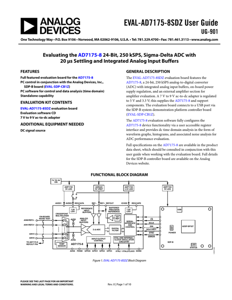
EVAL-AD7175-8SDZ User Guide UG-901 One Technology Way • P.O. Box 9106 • Norwood, MA 02062-9106, U.S.A. • Tel: 781.329.4700 • Fax: 781.461.3113 • www.analog.com Evaluating the AD7175-8 24-Bit, 250 kSPS, Sigma-Delta ADC with 20 µs Settling and Integrated Analog Input Buffers FEATURES GENERAL DESCRIPTION Full featured evaluation board for the AD7175-8 PC control in conjunction with the Analog Devices, Inc., SDP-B board (EVAL-SDP-CB1Z) PC software for control and data analysis (time domain) Standalone capability The EVAL-AD7175-8SDZ evaluation board features the AD7175-8, a 24-bit, 250 kSPS analog-to-digital converter (ADC) with integrated analog input buffers, on-board power supply regulation, and an external amplifier section for amplifier evaluation. A 7 V to 9 V ac-to-dc adapter is regulated to 5 V and 3.3 V; this supplies the AD7175-8 and support components. The evaluation board connects to a USB port via the SDP-B system demonstration platform controller board (EVAL-SDP-CB1Z). EVALUATION KIT CONTENTS EVAL-AD7175-8SDZ evaluation board Evaluation software CD 7 V to 9 V ac-to-dc adapter The AD7175-8 evaluation software fully configures the AD7175-8 device functionality via a user accessible register interface and provides dc time domain analysis in the form of waveform graphs, histograms, and associated noise analysis for ADC performance evaluation. ADDITIONAL EQUIPMENT NEEDED DC signal source Full specifications on the AD7175-8 are available in the product data sheet, which should be consulted in conjunction with this user guide when working with the evaluation board. Full details for the SDP-B controller board are available on the Analog Devices website. FUNCTIONAL BLOCK DIAGRAM 7V TO 9V VIN AVDD2 REGCAPA 1.8V LDO AIN0/REF2– ON-BOARD NOISE TEST CROSSPOINT MULTIPLEXER AVDD REF– IOVDD REF+ REFOUT BUFFERED PRECISION REFERENCE REFERENCE INPUT BUFFERS REGCAPD 1.8V LDO INT REF ANALOG INPUT BUFFERS Σ-Δ ADC DIGITAL FILTER CS SERIAL INTERFACE AND CONTROL SCLK DIN DOUT/RDY SYNC AIN15 AIN16 TEMP SENSOR XTAL AND INTERNA L CLOCK OSCILLATOR CIRCUITRY INPUT/OUTPUT CONTROL AVSS TO AD7175-8 REFOUT PIN USB AD7175-8 LED AIN1/REF2+ ADP7104 5V LDO ADSP-BF527 POWER ERROR SDP-B LED STATUS AVSS PDSW GPIO0 GPIO1 GPO2 GPO3 XTAL1 XTAL2/CLKIO DGND Figure 1. EVAL-AD7175-8SDZ Block Diagram PLEASE SEE THE LAST PAGE FOR AN IMPORTANT WARNING AND LEGAL TERMS AND CONDITIONS. Rev. 0 | Page 1 of 10 13767-001 AVDD1 ADP1720 3.3V LDO ADR445 5V VREF ADP1720 5V LDO UG-901 EVAL-AD7175-8SDZ User Guide TABLE OF CONTENTS Features .............................................................................................. 1 Power Supply Configurations ......................................................6 Evaluation Kit Contents ................................................................... 1 Analog Inputs.................................................................................6 Additional Equipment Needed ....................................................... 1 Reference Options .........................................................................6 General Description ......................................................................... 1 Evaluation Board Software ...............................................................7 Functional Block Diagram .............................................................. 1 Software Installation .....................................................................7 Revision History ............................................................................... 2 Launching the Software ................................................................7 EVAL-AD7175-8SDZ Quick Start Guide ...................................... 3 Software Operation ...........................................................................8 Recommended Quick Start Guide ............................................. 3 Overview of the Main Window ...................................................8 Quick Start Noise Test ................................................................. 3 Control Toolbar .............................................................................8 Evaluation Board Hardware ............................................................ 4 Data Section ...................................................................................9 Device Description ....................................................................... 4 Analysis Section .............................................................................9 Hardware Link Options ............................................................... 4 Status ...............................................................................................9 Sockets and Connectors .............................................................. 5 Exiting the Software ......................................................................9 Serial Interface .............................................................................. 5 Saving Results ................................................................................9 Power Supplies .............................................................................. 5 REVISION HISTORY 11/15—Revision 0: Initial Version Rev. 0 | Page 2 of 10 EVAL-AD7175-8SDZ User Guide UG-901 EVAL-AD7175-8SDZ QUICK START GUIDE RECOMMENDED QUICK START GUIDE QUICK START NOISE TEST Follow these steps to set up the board: Use the following procedure to quickly test the noise performance: 2. 3. 4. 5. 6. Disconnect the SDP-B board from the USB port of the PC. Install the AD7175-8 software from the enclosed CD. Restart the PC after installation. Connect the SDP-B board to the EVAL-AD7175-8SDZ evaluation board, as shown in Figure 2. Fasten the two boards together with the enclosed plastic screw washer set. Connect the external 9 V power supply to Connector J4 of the evaluation board, as shown in Figure 2. Set LK2 to Position B. Connect the SDP-B board to the PC via the USB cable. For Windows® XP, you may need to search for the SDP drivers. Choose to automatically search for the drivers for the SDP-B board if prompted by the operating system. From the Analog Devices subfolder in the Programs menu, launch the AD7175-8 software. 1. 2. Insert Link LK5 to Link LK20 to initiate the noise performance test mode. In this mode, analog input channels short to the REFOUT pin via SL11. In the evaluation software, click Start Sampling to acquire samples from the ADC (see Figure 7). The Samples numeric control in the top right corner of the main window sets the number of samples collected in each batch. 13767-002 1. Figure 2. Hardware Configuration, Setting Up the EVAL-AD7175-8SDZ Rev. 0 | Page 3 of 10 UG-901 EVAL-AD7175-8SDZ User Guide EVALUATION BOARD HARDWARE DEVICE DESCRIPTION HARDWARE LINK OPTIONS The AD7175-8 is a highly accurate, high resolution, multiplexed, 8-/16-channel (full/pseudo differential) Σ-Δ ADC. The AD7175-8 has a maximum channel-to-channel scan rate of 50 kSPS (20 µs) for fully settled data The output data rates range from 5 SPS to 250 kSPS. The device includes integrated analog input and reference buffers, an integrated precision 2.5 V reference, and an integrated oscillator. See Table 1 for the default link options. By default, the board is configured to operate from the supplied 9 V ac-to-dc adapter connected to Connector J4. The 5 V supply required for the AD7175-8 comes from the on-board low dropout regulator (LDO). The ADP1720, with a 5 V fixed output voltage, receives its input voltage from J2 or J4 (depending on the position of LK2) and generates a 5 V output. Table 1. Default Link and Solder Link Options Link LK1 Default Option A LK2 LK5 to LK20 B Inserted SL0 A SL1 A SL2 A SL3 A SL4 A SL5 B SL6 Removed SL7 A SL8 to SL9 SL10 A A SL11 A SL12 to SL15 Inserted Description Selects the voltage applied to the power supply sequencer circuit (U3); dependent on AVDD1. Place this link in Position A if using 5 V AVDD1, or Position B if using 2.5 V AVDD1. Selects the external power supply from Connector J3 (Position A), or J4 (Position B). Inserting these links sets up the on-board noise test. In this mode, all inputs short to the common voltage via SL11. Routes A0 to one of the following: Position A: AIN0/REF2− pin on the AD7175-8 Position B: Buffer U6 Position C: U7 for use with a single-ended to differential driver circuit Position D: J15-1 Routes A1 to one of the following: Position A: AIN1/REF2+ pin on the AD7175-8 Position B: Buffer U6 Position C: U7 for use with a single-ended to differential driver circuit Position D: J15-7 Routes A2 to one of the following: Position A: AIN2 pin on the AD7175-8 Position B: Buffer U10 Position C: U9 for use with a single-ended to differential driver circuit Routes A3 to one of the following: Position A: AIN3 pin on the AD7175-8 Position B: Buffer U10 Position C: U9 for use with a single-ended to differential driver circuit Sets the voltage applied to the AVDD2 pin. Operates using the AVDD1 supply (default). Position B sets the AVDD2 voltage to the 3.3 V supply from the ADP1720 3.3 V regulator (U11). Selects between an external or on-board IOVDD source. Supplies IOVDD from the ADP1720 3.3 V regulator (U11) (default). The evaluation board operates with a 3.3 V logic. Position A connects Crystal Y1 as an external MCLK clock source. Position B connects the MCLK SMA/SMB connector for use as a clock input or an ADC internal clock output. Selects between an external or on-board AVDD1 source. Supplies AVDD1 from the ADP1720 5 V regulator (U8) (default). Selects between a 5 V and 2.5 V LDO supply for AVDD1. Supplies AVDD1 with 5 V (default). Selects the voltage applied to the AVDD1 pin. Operates using the supply set up by Link SL8 to Link SL9 (default). When inserted in Position B, sets the AVDD1 voltage to the 3.3 V supply from the ADP1720 3.3 V regulator. Selects the voltage applied to analog input during on-board noise test (LK5 to LK20 inserted). Position A connects to the AD7175-8 REFOUT pin. Position B connects to GND. Position C connects to AVSS. Connects AVSS and AGND for single-supply operation. To operate in split supply mode, remove these links. Rev. 0 | Page 4 of 10 EVAL-AD7175-8SDZ User Guide UG-901 SOCKETS AND CONNECTORS Table 2. Connector Details Connector J1 Function Connector to the EVAL-SDP-CB1Z A0 to A3 Analog inputs to the ADC J3 External bench top voltage supply for the EVAL-AD7175-8SDZ External ac-to-dc adapter input for the EVAL-AD7175-8SDZ, 7 V to 9 V J4 J5 J8 J10 and J12 J14 External bench top voltage supply option for AVDD1/AVDD2 and IOVDD inputs on the AD7175-8 GPIO terminal J15 Analog input terminal block; wired connection to external source or sensor Analog input terminal block; wired connection to external source or sensor Optional header J16 Optional header 1 Connector Type 120-way connector, 0.6 mm pitch Straight PCB mount SMB/SMA jack Power socket block, 3-pin, 3.81 mm pitch DC power connectors, 2 mm SMT power jack Screw terminal block, 3.81 mm pitch Manufacturer Hirose Manufacturer Number FX8-120S-SV(21) Order Code1 FEC1324660 Tyco 1-1337482-0 Not applicable Phoenix Contact Kycon MC 1,5/ 3-G-3,81 FEC3704757 KLDX-SMT20202-A MOUSER 806KLDX-SMT20202A Phoenix Contact MKDS 1/4-3.81 FEC3704592 Power socket block, 4-pin, 3.81 mm pitch Power socket block, 8-pin, 3.81 mm pitch Power socket block, 6-pin, 3.81 mm pitch 7-way, 2.54 mm pin header 7-way, 2.54 mm socket Phoenix Contact Phoenix Contact Phoenix Contact Samtec MC 1,5/ 4-G-3,81 FEC3704749 MC 1,5/ 8-G-3,81 FEC3704774 MC 1,5/ 6-G-3,81 FEC3704762 SSW-107-01-T-S FEC1803478 Samtec TLW-107-05-G-S FEC1668499 Order codes starting with FEC are for Farnell. SERIAL INTERFACE POWER SUPPLIES The EVAL-AD7175-8SDZ evaluation board connects to the Blackfin® ADSP-BF527 on the SDP-B controller board via the serial peripheral interface (SPI). There are four primary signals, CS, SCLK, and DIN (all inputs), and one output from the ADC, DOUT/RDY. Power the evaluation board from the ac-to-dc adapter connected to J4, or from an external bench top supply applied to J3 or J5. Linear LDOs generate the required voltages from the applied input voltage (VIN) rail when using J3 or J4. Use J5 to bypass the on-board regulators. The regulators used are the 5 V fixed output voltage and 2.5 V adjustable output voltage ADP1720 devices, which supply the AVDD1 and AVDD2 rails to the ADC; the ADP1720 (3.3 V) supplies the IOVDD rail. Use the ADP7104 (5 V) to supply 5 V for the SDP-B controller board. Each supply is decoupled where it enters the board and again at each device. Table 3 shows the various power supply configurations available, including split supply operation. To operate the evaluation board in standalone mode, disconnect the AD7175-8 serial interface lines from the 120-pin header by removing the 0 Ω, R9 through R13 links. Use the test points to connect the signals to an alternative digital capture setup. Rev. 0 | Page 5 of 10 UG-901 EVAL-AD7175-8SDZ User Guide Table 3. Power Supply Configurations1 Configuration Single Supply (Regulated) Single Supply (Unregulated) Split Supply (Regulated) Split Supply (Unregulated) 1 Input Voltage Range 7 V to 9 V 7 V to 9 V, 5 V, and 3.3 V 7 V to 9 V and −2.5 V 7 V to 9 V, ±2.5 V, and 3.3 V Description The 7 V to 9 V input is regulated to 5 V for AVDD1/AVDD2 and 3.3 V for IOVDD. This supply also powers the external 5 V reference. See the Single Supply (Regulated) section. The input is unregulated and connects directly to AVDD1/AVDD2 and IOVDD from J5. The 7 V to 9 V input powers the external 5 V reference. See the Single Supply (Unregulated) section . The 7 V to 9 V input is regulated to 2.5 V for AVDD1/AVDD2 and 3.3 V for IOVDD. The 7 V to 9 V input powers the external 5 V reference, and the −2.5 V input is connected to AVSS directly (unregulated). See the Split Supply (Regulated) section. The input is unregulated and connects directly to AVDD1/AVDD2 and IOVDD from J5. The 7 V to 9 V input powers the external 5 V reference. See the Split Supply (Unregulated) section. Only one configuration can be used at a time. Split Supply (Unregulated) POWER SUPPLY CONFIGURATIONS Single Supply (Regulated) To set up the board, use the following procedure: There are two available power supply options for the singlesupply (regulated) configuration. 1. 2. 3. 4. 5. 6. 7. • • An ac-to-dc adapter (included) connected to J4. Set LK2 to Position B. A bench top power supply connected to J3. Set LK2 to Position A and ensure that AVSS = AGND = 0 V. Set all other links and solder links to the default settings as outlined in Table 1. 8. Single Supply (Unregulated) To set up the board, use the following procedure: 1. 2. 3. 4. 5. 6. Move SL5 to Position A and SL7 to Position B. Connect the two terminals of J5 labeled AGND and AVSS. Connect 0 V (GND) to J5 at the terminal labeled AGND. Connect 5 V to J5 at the terminal labeled AVDD. Connect 3.3 V to J5 at the terminal labeled IOVDD. Connect the 7 V to 9 V input to either J3 or J4. Set all other links and solder links to the default settings as outlined in Table 1. Split Supply (Regulated) To set up the board, use the following procedure: 1. 2. 3. Remove SL12 to SL15. These links connect AVSS to AGND. Connect a bench top power supply to J3 and set LK2 to Position A. Make sure that AVSS = −2.5 V in this case. Set LK1 to Position B. This sets the input to the power monitor circuitry to work with the lower AVDD1 supply of 2.5 V. Set all other links and solder links to the default settings as outlined in Table 1. Move SL5 to Position A and move SL7 to Position B. Remove SL12 to SL15. Connect 0 V (GND) to J5 at the terminal labeled AGND. Connect 2.5 V to J5 at the terminal labeled AVDD. Connect −2.5 V to J5 at the terminal labeled AVSS. Connect 3.3 V to J5 at the terminal labeled IOVDD. Connect 7 V to 9 V to either J3 or J4. Connect or disconnect the AVSS terminal of J3 to the AVSS terminal of J5. Set LK1 to Position B. This sets the input to the power monitor circuitry to work with the lower AVDD1 supply of 2.5 V. Set all other links and solder links set to the default settings as outlined in Table 1. ANALOG INPUTS The EVAL-AD7175-8SDZ primary analog inputs can be applied in two separate ways: • • J10, J12, and J14 connectors on the left side of the board A0 to A3 SMB/SMA footprints on the evaluation board The analog inputs route directly to the associated analog input pins on the AD7175-8, provided that the LK5 to LK20 links (on-board noise test) are removed. The AD7175-8 evaluation software is set up to analyze dc inputs to the ADC. The AD7175-8 input buffers work for dc input signals. REFERENCE OPTIONS The EVAL-AD7175-8SDZ includes an external 5 V reference, the ADR445. The AD7175-8 includes an internal 2.5 V reference. The default operation is to use the external reference input, which is set to accept the 5 V ADR445 on the evaluation board. Choose the reference in the SETUPCONx registers associated with Setup 0 to Setup 7 to select the reference used for conversions by the AD7175-8. Change between the internal and external references by accessing the AD7175-8 register map in the evaluation software (click ADC Setup). Rev. 0 | Page 6 of 10 EVAL-AD7175-8SDZ User Guide UG-901 EVALUATION BOARD SOFTWARE Take the following steps to verify that the SDP-B controller board driver is installed and working correctly: SOFTWARE INSTALLATION The EVAL-AD7175-8SDZ evaluation kit includes software on a CD. Double-click the setup.exe file from the CD to run the installer. The default installation location for the software is C:\Program Files\Analog Devices\EVAL-AD7175-8SDZ\. 1. 2. Install the evaluation software before connecting the evaluation board and SDP-B controller board to the USB port of the PC to ensure that the evaluation system is correctly recognized when connected to the PC. 3. There are two parts to the installation: Allow the Found New Hardware Wizard to run. After the drivers are installed, check that the board has connected correctly by looking at the Device Manager of the PC. The Device Manager can be found by right clicking My Computer, selecting Manage, and then Device Manager from the list of System Tools (see Figure 5). The SDP-B board appears under ADI Development Tools as Analog Devices System Development Platform or similar. The installation is complete. AD7175-8 evaluation board software installation EVAL-SDP-CB1Z SDP-B board drivers installation 13767-005 Place the software and drivers in the appropriate locations by proceeding through all of the installation steps. Connect the SDP-B board to the PC only after the software and drivers are installed. The installer may prompt for permission to allow the program to make changes to the computer. Click Yes to proceed (see Figure 3). Figure 5. Device Manager LAUNCHING THE SOFTWARE The AD7175-8 software can be launched when the EVALAD7175-8SDZ evaluation board and the EVAL-SDP-CB1Z SDP-B controller board are correctly connected to the PC. 13767-003 To launch the software, do the following: 1. Figure 3. User Account Control Permission Dialog Box 2. 13767-004 A security warning may appear as part of the SDP-B controller board driver installation. Click Install to proceed with the installation of the driver (see Figure 4). Without this confirmation, the software cannot operate correctly. From the Start menu, click Programs, Analog Devices, and then EVAL-AD7175-8SDZ. The main window of the software then displays (see Figure 7). If the AD7175-8 evaluation system is not connected to the USB port via the SDP-B board when the software is launched, a connectivity error displays (see Figure 6). Connect the evaluation board to the USB port of the PC, wait a few seconds, click Rescan, and follow the instructions. After installation is complete, connect the EVAL-AD7175-8SDZ evaluation board to the EVAL-SDP-CB1Z SDP-B board, as shown in Figure 2. Connect the SDP-B board via the USB cable to the computer. Rev. 0 | Page 7 of 10 13767-006 Figure 4. SDP-B Drivers Installation Confirmation Dialog Box Figure 6. Connectivity Error Alert Dialog Box UG-901 EVAL-AD7175-8SDZ User Guide SOFTWARE OPERATION 1 2 13767-007 3 4 Figure 7. Main Window of the AD7175-8 Evaluation Software OVERVIEW OF THE MAIN WINDOW Sampling The main window of the software displays the significant control buttons and analysis indicators of the AD7175-8 evaluation software (see Figure 7). This window is divided into four sections. The green numbers shown in Figure 7 (Label 1 through Label 4) correspond to the following components of the main window: Sampling (set to Capture in Figure 7) enacts the sampling mode used by the software. This is unrelated to the ADC mode. The user can capture a defined sample set or continuously gather batches of samples. In both cases, the number of samples set in the Samples numeric input dictates the number of samples. Click ADC Setup to open the ADC register map window. Use the new window to change register settings. This window allows the user to save existing register settings or load previously saved register settings. Control toolbar (Label 1)—control buttons Data section (Label 2)—waveform graph and controls Analysis section (Label 3)—histogram graph and controls Status bar (Label 4)—information ADC Setup CONTROL TOOLBAR ADC Reset Start Sampling and Samples Click ADC Reset to perform a software reset of the AD7175-8. There is no hardware reset pin. Perform a hard reset by removing power to the board. The software reset has the same effect as a hard reset. Start Sampling, located on the right of the control toolbar, gathers ADC results. Results appear in the graphs of the DATA and ANALYSIS sections of the main window. The Samples numeric control is the number of samples gathered per batch. Delete Data Clear Graphs Click Delete Data Clear Graphs to clear any existing content from the waveform and histogram graphs. Rev. 0 | Page 8 of 10 EVAL-AD7175-8SDZ User Guide UG-901 DATA SECTION ANALYSIS SECTION Data Waveform Analysis Histogram and Analysis Channel The data waveform shows each successive sample of the ADC output. The toolbar in the graph allows the user to zoom in on the data. Change the scales on the graph by typing values into the x-axis and y-axis. The histogram shows the analysis of the channel selected via the analysis channel drop-down box. This graph only shows the histogram for one channel at a time. Display Units Click Display Units to select whether the data graph displays in units of voltages or codes. This is the number of samples used for creating the histogram analysis. This is automatically set to equal the number of samples when Start Sampling is clicked. Vref Analysis Results Vref sets the reference voltage used for calculating the results on the data graph. The user must update this value when the reference source changes, because it does not automatically update. This section displays the results of the histogram analysis for the selected analysis channel. This includes both noise and resolution measurements. Autoscale STATUS Autoscale enables and disables the y-axis autoscale control for the data graph. With this control enabled, the graph automatically sets the maximum and minimum y-axis values to fit the displayed data. The status section at the bottom of the window display status updates such as Analysis Completed and Reset Completed during software use. X-scale and X-scale Samples EXITING THE SOFTWARE These controls set the number of data points displayed on the x-axis. When set to fixed, the number of data points is equal to the number in the X-scale Samples numeric input. This control automatically updates each time Start Sampling is clicked. When set to dynamic, all samples are displayed, including those from previous sample batches. To exit the software, click the close button at the top, right corner of the main window (see Figure 7). Channel Selection 1. 2. 3. This control allows the user to choose which channels display on the data waveform. It also shows the analog inputs for that channel labeled next to the on and off controls. These controls only affect the display of the channels and do not have any effect on the channel settings in the ADC register map. Latest Data Analyse Last # Samples SAVING RESULTS The software can save the current captured data for later analysis. 4. Right-click the waveform graph. Click Export in the drop-down menu. Select the folder for the data to be saved into and the name of the file you want to save. Click Save. The data is saved in the format selected for display units via the Display Units option. These indicators show the value of the last sample gathered on the corresponding channel (see Channel Selection). Rev. 0 | Page 9 of 10 UG-901 EVAL-AD7175-8SDZ User Guide NOTES ESD Caution ESD (electrostatic discharge) sensitive device. Charged devices and circuit boards can discharge without detection. Although this product features patented or proprietary protection circuitry, damage may occur on devices subjected to high energy ESD. Therefore, proper ESD precautions should be taken to avoid performance degradation or loss of functionality. Legal Terms and Conditions By using the evaluation board discussed herein (together with any tools, components documentation or support materials, the “Evaluation Board”), you are agreeing to be bound by the terms and conditions set forth below (“Agreement”) unless you have purchased the Evaluation Board, in which case the Analog Devices Standard Terms and Conditions of Sale shall govern. Do not use the Evaluation Board until you have read and agreed to the Agreement. Your use of the Evaluation Board shall signify your acceptance of the Agreement. This Agreement is made by and between you (“Customer”) and Analog Devices, Inc. (“ADI”), with its principal place of business at One Technology Way, Norwood, MA 02062, USA. Subject to the terms and conditions of the Agreement, ADI hereby grants to Customer a free, limited, personal, temporary, non-exclusive, non-sublicensable, non-transferable license to use the Evaluation Board FOR EVALUATION PURPOSES ONLY. Customer understands and agrees that the Evaluation Board is provided for the sole and exclusive purpose referenced above, and agrees not to use the Evaluation Board for any other purpose. Furthermore, the license granted is expressly made subject to the following additional limitations: Customer shall not (i) rent, lease, display, sell, transfer, assign, sublicense, or distribute the Evaluation Board; and (ii) permit any Third Party to access the Evaluation Board. As used herein, the term “Third Party” includes any entity other than ADI, Customer, their employees, affiliates and in-house consultants. The Evaluation Board is NOT sold to Customer; all rights not expressly granted herein, including ownership of the Evaluation Board, are reserved by ADI. CONFIDENTIALITY. This Agreement and the Evaluation Board shall all be considered the confidential and proprietary information of ADI. Customer may not disclose or transfer any portion of the Evaluation Board to any other party for any reason. Upon discontinuation of use of the Evaluation Board or termination of this Agreement, Customer agrees to promptly return the Evaluation Board to ADI. ADDITIONAL RESTRICTIONS. Customer may not disassemble, decompile or reverse engineer chips on the Evaluation Board. Customer shall inform ADI of any occurred damages or any modifications or alterations it makes to the Evaluation Board, including but not limited to soldering or any other activity that affects the material content of the Evaluation Board. Modifications to the Evaluation Board must comply with applicable law, including but not limited to the RoHS Directive. TERMINATION. ADI may terminate this Agreement at any time upon giving written notice to Customer. Customer agrees to return to ADI the Evaluation Board at that time. LIMITATION OF LIABILITY. THE EVALUATION BOARD PROVIDED HEREUNDER IS PROVIDED “AS IS” AND ADI MAKES NO WARRANTIES OR REPRESENTATIONS OF ANY KIND WITH RESPECT TO IT. ADI SPECIFICALLY DISCLAIMS ANY REPRESENTATIONS, ENDORSEMENTS, GUARANTEES, OR WARRANTIES, EXPRESS OR IMPLIED, RELATED TO THE EVALUATION BOARD INCLUDING, BUT NOT LIMITED TO, THE IMPLIED WARRANTY OF MERCHANTABILITY, TITLE, FITNESS FOR A PARTICULAR PURPOSE OR NONINFRINGEMENT OF INTELLECTUAL PROPERTY RIGHTS. IN NO EVENT WILL ADI AND ITS LICENSORS BE LIABLE FOR ANY INCIDENTAL, SPECIAL, INDIRECT, OR CONSEQUENTIAL DAMAGES RESULTING FROM CUSTOMER’S POSSESSION OR USE OF THE EVALUATION BOARD, INCLUDING BUT NOT LIMITED TO LOST PROFITS, DELAY COSTS, LABOR COSTS OR LOSS OF GOODWILL. ADI’S TOTAL LIABILITY FROM ANY AND ALL CAUSES SHALL BE LIMITED TO THE AMOUNT OF ONE HUNDRED US DOLLARS ($100.00). EXPORT. Customer agrees that it will not directly or indirectly export the Evaluation Board to another country, and that it will comply with all applicable United States federal laws and regulations relating to exports. GOVERNING LAW. This Agreement shall be governed by and construed in accordance with the substantive laws of the Commonwealth of Massachusetts (excluding conflict of law rules). Any legal action regarding this Agreement will be heard in the state or federal courts having jurisdiction in Suffolk County, Massachusetts, and Customer hereby submits to the personal jurisdiction and venue of such courts. The United Nations Convention on Contracts for the International Sale of Goods shall not apply to this Agreement and is expressly disclaimed. ©2015 Analog Devices, Inc. All rights reserved. Trademarks and registered trademarks are the property of their respective owners. UG13767-0-11/15(0) Rev. 0 | Page 10 of 10
