Circuit Note CN-0051
advertisement

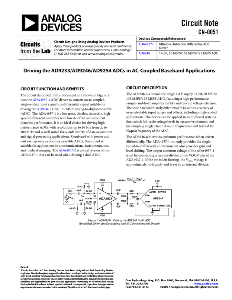
Circuit Note CN-0051 Circuit Designs Using Analog Devices Products Apply these product pairings quickly and with confidence. For more information and/or support call 1-800-AnalogD (1-800-262-5643) or visit www.analog.com/circuits. Devices Connected/Referenced ADA4937-1 Ultralow Distortion Differential ADC Driver AD9246 14-Bit, 80 MSPS/105 MSPS/125 MSPS ADC Driving the AD9233/AD9246/AD9254 ADCs in AC-Coupled Baseband Applications CIRCUIT FUNCTION AND BENEFITS CIRCUIT DESCRIPTION The circuit described in this document and shown in Figure 1 uses the ADA4937-1 ADC driver to convert an ac-coupled, single-ended input signal to a differential signal suitable for driving the AD9246 14-bit, 125 MSPS analog-to-digital converter (ADC). The ADA4937-1 is a low noise, ultralow distortion, high speed differential amplifier with low dc offset and excellent dynamic performance. It is an ideal choice for driving high performance ADCs with resolutions up to 16 bits from dc to 100 MHz and is well suited for a wide variety of data acquisition and signal processing applications. Combined with power and cost savings over previously available ADCs, this circuit is suitable for applications in communications, instrumentation, and medical imaging. The ADA4937-2 is a dual version of the ADA4937-1 that can be used when driving a dual ADC. The AD9246 is a monolithic, single 1.8 V supply, 14-bit, 80 MSPS/ 105 MSPS/125 MSPS ADC, featuring a high performance sample-and-hold amplifier (SHA) and on-chip voltage reference. The wide bandwidth, truly differential SHA allows a variety of user-selectable input ranges and offsets, including single-ended applications. The device can be applied in multiplexed systems that switch full-scale voltage levels in successive channels and for sampling single-channel input frequencies well beyond the Nyquist frequency of the ADC. 200Ω 49.9Ω 10µF 90.9Ω VIN 10µF (VIN+) – (VIN–) =2 VIN 1.8V 33Ω + +IN VOCM 90.9Ω –IN 200Ω ADA4937 10pF 200Ω 10µF 76.8Ω AVDD VIN– DRVDD AD9246 VIN+ 33Ω AGND SENSE CML 08610-001 VIN 10µF GAIN = 5V 76.8Ω 50Ω The AD9246 achieves its optimum performance when driven differentially. The ADA4937-1 not only provides the singleended-to-differential conversion but also provides gain and level shifting. The output common voltage of the ADA4937-1 is set by connecting a resistive divider to the VOCM pin of the ADA4937-1. If the pin is left floating, the VOCM voltage is approximately midsupply and is set by an internal divider. 200Ω Figure 1. ADA4937-1 Driving the AD9246 14-Bit ADC (Simplified Schematic: Decoupling and All Connections Not Shown) Rev. A “Circuits from the Lab” from Analog Devices have been designed and built by Analog Devices engineers. Standard engineering practices have been employed in the design and construction of each circuit, and their function and performance have been tested and verified in a lab environment at room temperature. However, youare solely responsible for testing the circuit and determining its suitability and applicability for your use and application. Accordingly, in no event shall Analog Devices be liable for direct, indirect, special, incidental, consequential or punitive damages due to any cause whatsoever connected to the use of any“Circuit fromthe Lab”. (Continued on last page) One Technology Way, P.O. Box 9106, Norwood, MA 02062-9106, U.S.A. Tel: 781.329.4700 www.analog.com Fax: 781.461.3113 ©2009 Analog Devices, Inc. All rights reserved. CN-0051 Circuit Note The ADA4937-1 is powered with a single 5 V supply and is configured for a gain-of-2 for a single-ended, input-to-differential output. The 76.8 Ω termination resistor, in parallel with the single-ended input impedance of 137 Ω, provides a 50 Ω ac termination for the source. The additional 49.9 Ω resistor, 10 µF capacitor, and 76.8 Ω resistor connected to the 90.9 Ω resistor on the inverting input balance the ac impedance driving the noninverting input. A detailed analysis of this configuration can be found in MT-076 Tutorial. The signal generator has a symmetric, ground-referenced, bipolar output. The VOCM pin of the ADA4937-1 is left unconnected; therefore, the internal divider sets the output common-mode voltage to midsupply. A portion of this is fed back to the summing nodes, biasing −IN and +IN at 1.14 V. For a common-mode voltage of 2.5 V, each ADA4937-1 output swings between 2.0 V and 3.0 V, providing a 2 V p-p differential output for a 1 V p-p single-ended input. The output of the ADC driver is ac-coupled to a single-pole, low-pass noise filter. The low-pass filter reduces the noise bandwidth at the ADC input and provides a degree of isolation from the switched capacitor inputs of the ADC and the driver. In any configuration, the optimum value of the shunt capacitor, C, is dependent on the input frequency and source impedance and may need to be optimized. Table 1 displays recommended values for the RC network. However, these values are dependent on the input signal frequency and may require further optimization. The input common-mode voltage to the ADC is set by the CML pin of the AD9246 and the pair of 200 Ω resistors. In other applications, the CML pin of the ADC and the VOCM pin of the ADA4937-1 are used to set the input common-mode voltage to the ADC (see the Common Variations section). The ADA4937-1 is fabricated using the Analog Devices, Inc., proprietary silicongermanium (SiGe), complementary bipolar process, enabling it to achieve very low levels of distortion with an input voltage noise of only 2.2 nV/ √Hz. The circuit shown in Figure 1 was tested with a −1 dBFS signal at various input frequencies. Figure 2 shows a plot of the second and third harmonic distortion (HD2/HD3) vs. input frequency. –75 –80 HD3 It is required that the exposed pad on the underside of both the AD9246 and the ADA4937-1 (LFCSP packages) be connected to a large area ground plane to achieve the best electrical and thermal performance. The copper plane should have several vias to achieve the lowest possible resistive thermal path for heat dissipation to flow through the bottom of the PCB. These vias should be solder filled or plugged. COMMON VARIATIONS The AD9246 (14-bit, 80 MSPS/105 MSPS/125 MSPS) ADC is pin compatible with both the AD9233 (12-bit, 80 MSPS/105 MSPS/ 125 MSPS) and the AD9254 (14-bit, 150 MSPS). There are a few other amplifier configurations to consider when driving ADCs. They are differential ac-coupled input to differential output, dc-coupled single-ended input to ac-coupled differential output, dc-coupled single-ended input to differential output, and dc-coupled differential input to differential output. In dc-coupled systems, the driver output common-mode voltage is set via the VOCM pin of the ADA4937-1. The adjustable level of the output common-mode voltage allows the ADA4937-1 output to match the input common-mode voltage of the ADC. The internal common-mode feedback loop of the ADA4937-1 also provides exceptional output balance and suppression of even-order harmonic distortion products. Often in these applications, the ADC CML pin is connected directly to the VOCM pin of the driver to ensure that optimal ADC input common-mode voltage is achieved. In other applications, the VOCM pin can be driven from a low impedance source such as an op amp. It can also be left floating but bypassed with a capacitor; in this case the VOCM voltage is set at the midpoint of the voltage applied to the two supply pins. Table 1. RC Network Recommended Values Input Frequency Range (MHz) R Series ( Ω) C Differential (pF) 0 to 70 33 15 70 to 200 33 5 200 to 300 15 5 >300 15 Open (no capacitor) –85 HD2 –90 –95 –100 0 20 40 60 80 FREQUENCY (MHz) 100 120 08610-002 HARMONIC DISTORTION (dBc) G = +2 The circuit must be constructed on a multilayer PC board with a large area ground plane. Proper layout, grounding, and decoupling techniques must be used to achieve optimum performance (see MT-031 Tutorial, MT-101 Tutorial, and the AD9246 evaluation board layout). Figure 2. Second Harmonic Distortion (HD2) and Third Harmonic Distortion (HD3) for the ADA4937-1 Driving the AD9246 ADC Rev. A | Page 2 of 3 Circuit Note CN-0051 LEARN MORE Data Sheets and Evaluation Boards Rob Reeder and Jim Caserta, Wideband A/D Converter FrontEnd Design Considerations II: Amplifier- or Transformer Drive for the ADC? Ask The Application Engineer—36, Analog Dialogue 41-02, February 2007. ADA4937-1 Data Sheet. AD9246 Data Sheet AD9246 Evaluation Board. MT-031 Tutorial, Grounding Data Converters and Solving the Mystery of "AGND" and "DGND," Analog Devices. REVISION HISTORY MT-074 Tutorial, Differential Drivers for Precision ADCs, Analog Devices. Updated Format ................................................................. Universal 11/09—Rev. 0 to Rev. A 2/09—Revision 0: Initial Release MT-075 Tutorial, Differential Drivers for High Speed ADCs Overview, Analog Devices. MT-076 Tutorial, Differential Driver Analysis, Analog Devices. MT-101 Tutorial, Decoupling Techniques, Analog Devices. John Ardizonni and Jonathan Pearson, "Rules of the Road" for High-Speed Differential ADC Drivers, Analog Dialogue, Volume 43, May 2009, Analog Devices. ADIsimDiffAmp (Differential Amplifier Tool), Analog Devices. (Continued from first page) "Circuits from the Lab" are intended only for use with Analog Devices products and are the intellectual property of Analog Devices or its licensors. While you may use the "Circuits from the Lab" in the design of your product, no other license is granted by implication or otherwise under any patents or other intellectual property by application or use of the "Circuits from the Lab". Information furnished by Analog Devices is believed to be accurate and reliable. However, "Circuits from the Lab" are supplied "as is" and without warranties of any kind, express, implied, or statutory including, but not limited to, any implied warranty of merchantability, noninfringement or fitness for a particular purpose and no responsibility is assumed by Analog Devices for their use, nor for any infringements of patents or other rights of third parties that may result from their use. Analog Devices reserves the right to change any "Circuits from the Lab" at any time without notice, but is under no obligation to do so. Trademarks and registered trademarks are the property of their respective owners. ©2009 Analog Devices, Inc. All rights reserved. Trademarks and registered trademarks are the property of their respective owners. CN08610-0-11/09(A) Rev. A | Page 3 of 3


